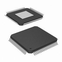
HMP8117CNZ Intersil, HMP8117CNZ Datasheet - Page 36

HMP8117CNZ
Manufacturer Part Number
HMP8117CNZ
Description
IC VIDEO DECODER NTSC/PAL 80PQFP
Manufacturer
Intersil
Type
Video Decoderr
Datasheet
1.HMP8117CNZ.pdf
(45 pages)
Specifications of HMP8117CNZ
Applications
Video
Voltage - Supply, Analog
4.75 V ~ 5.25 V
Voltage - Supply, Digital
4.75 V ~ 5.25 V
Mounting Type
Surface Mount
Package / Case
80-MQFP, 80-PQFP
Lead Free Status / RoHS Status
Lead free / RoHS Compliant
Available stocks
Company
Part Number
Manufacturer
Quantity
Price
NO.
NO.
NO.
NO.
NO.
BIT
BIT
BIT
BIT
BIT
7-0
7-0
7-0
5-3
2-0
7-0
7
6
Negate BLANK
Output Signal
Negate HSYNC
Output Signal
Horizontal Sync
Detect Window
MV Stripe Detection
and Bypass Enable
MV PSP Detection
Enable
MV PSP Detection
Count
MV Detection
Field Count
Reserved
FUNCTION
FUNCTION
FUNCTION
FUNCTION
FUNCTION
36
This 8-bit register specifies the line number to negate BLANK each field.
For NTSC operation, it occurs on line (n + 5) on odd fields and line (n + 268) on even fields. For
PAL operation, it occurs on line (n + 5) on odd fields and line (n + 318) on even fields.
This 8-bit register specifies the horizontal count at which to negate HSYNC each scan line.
Values may range from 0 (0000 0000) to 510 (1111 1111) CLK2 cycles. The leading edge of
HSYNC is count 00
This 8-bit register specifies the width of the timing window (in 1x clock samples) for the digital
PLL to accept horizontal sync pulses in each line. The window is centered about where the
horizontal sync pulse should be located.
If the horizontal sync pulse falls inside the window, the digital PLL maintains normal lock timing.
If the horizontal sync pulse falls outside this window, the digital PLL will to enter the horizontal
lock acquisition mode based on the current setting for bits 3-2 of register 04
changing this register to 90
video sources.
Set to “1” to enable the detection and bypass of the MV Color Striping component. If this bit is
not enabled and the MV Color Striping component exists on the input signal, artifacts will be
clearly visible as horizontal streaks in the output data. This bit must be enabled for the MV
Detection Status of register 0E
Set to “1” to enable detection of the MV Pseudo Sync Pulse (PSP)
component. If the MV PSP component exists on the input signal, this bit must be enabled for the
MV Detection Status of register 0E
Defines the number of extra sync pulses required before declaring the Pseudo Sync Pulse (PSP)
component in the MV Detection Status of register 0E
present for the number of fields defined in bits 2-0 below.
Defines the minimum number of fields that an MV component must be present for in order to
change the MV Detection Status of register 0E
count. Ex: The default of 110
Set bits 5-4 to 11
TABLE 59. HSYNC DETECT WINDOW REGISTER
TABLE 57. END V_BLANK REGISTER
B
TABLE 58. END HSYNC REGISTER
for optimum performance.
H
.
TABLE 60. MV CONTROL
TABLE 61. RESERVED
SUB ADDRESS = 35
SUB ADDRESS = 36
SUB ADDRESS = 37
SUB ADDRESS = 41
SUB ADDRESS = 42
H
B
HMP8117
following reset in order to widen the window for poorly timed input
H
is actually 6 + 2 = 8 fields.
to be updated.
H
to be updated.
DESCRIPTION
DESCRIPTION
DESCRIPTION
DESCRIPTION
DESCRIPTION
H
H
H
H
H
H
. Add 2 to bits 2-0 to obtain the minimum field
H
. The PSP component must also be
H
. Recommend
(Use 90
(Use 30
April 19, 2007
RESET
RESET
RESET
RESET
RESET
STATE
STATE
STATE
STATE
STATE
100
110
12
30
20
00
0
0
FN4643.3
B
B
H
H
H
H
B
B
H
H
)
)


