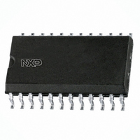
PCA9539D,118 NXP Semiconductors, PCA9539D,118 Datasheet - Page 5

PCA9539D,118
Manufacturer Part Number
PCA9539D,118
Description
IC I/O EXPANDER I2C 16B 24SOIC
Manufacturer
NXP Semiconductors
Datasheet
1.PCA9539BS118.pdf
(31 pages)
Specifications of PCA9539D,118
Package / Case
24-SOIC (7.5mm Width)
Interface
I²C, SMBus
Number Of I /o
16
Interrupt Output
Yes
Frequency - Clock
400kHz
Voltage - Supply
2.3 V ~ 5.5 V
Operating Temperature
-40°C ~ 85°C
Mounting Type
Surface Mount
Includes
POR
Logic Family
PCA9539
Number Of Lines (input / Output)
16.0 / 16.0
Operating Supply Voltage
2.3 V to 5.5 V
Power Dissipation
200 mW
Operating Temperature Range
- 40 C to + 85 C
Input Voltage
5 V
Logic Type
I2C, SMBus
Maximum Clock Frequency
400 KHz
Mounting Style
SMD/SMT
Number Of Input Lines
16.0
Number Of Output Lines
16.0
Output Current
50 mA
Output Voltage
5 V
Lead Free Status / RoHS Status
Lead free / RoHS Compliant
Lead Free Status / RoHS Status
Lead free / RoHS Compliant, Lead free / RoHS Compliant
Other names
568-1842-2
935277297118
PCA9539D-T
935277297118
PCA9539D-T
NXP Semiconductors
PCA9539_PCA9539R_5
Product data sheet
5.2 Pin description
Table 3.
[1]
Symbol
INT
A1
RESET
IO0_0
IO0_1
IO0_2
IO0_3
IO0_4
IO0_5
IO0_6
IO0_7
V
IO1_0
IO1_1
IO1_2
IO1_3
IO1_4
IO1_5
IO1_6
IO1_7
A0
SCL
SDA
V
SS
DD
HVQFN24 package die supply ground is connected to both V
be connected to supply ground for proper device operation. For enhanced thermal, electrical, and board
level performance, the exposed pad needs to be soldered to the board using a corresponding thermal pad
on the board and for proper heat conduction through the board, thermal vias need to be incorporated in the
PCB in the thermal pad region.
Pin description
Pin
SO24, TSSOP24
1
2
3
4
5
6
7
8
9
10
11
12
13
14
15
16
17
18
19
20
21
22
23
24
16-bit I
2
Rev. 05 — 28 July 2008
C-bus and SMBus low power I/O port with interrupt and reset
HVQFN24
22
23
24
1
2
3
4
5
6
7
8
9
10
11
12
13
14
15
16
17
18
19
20
21
[1]
PCA9539; PCA9539R
Description
interrupt output (open-drain)
address input 1
active LOW reset input. Driving this pin LOW
causes:
port 0 input/output 0
port 0 input/output 1
port 0 input/output 2
port 0 input/output 3
port 0 input/output 4
port 0 input/output 5
port 0 input/output 6
port 0 input/output 7
supply ground
port 1 input/output 0
port 1 input/output 1
port 1 input/output 2
port 1 input/output 3
port 1 input/output 4
port 1 input/output 5
port 1 input/output 6
port 1 input/output 7
address input 0
serial clock line input
serial data line open-drain input/output
supply voltage
•
•
PCA9539 to reset its state machine and
registers
PCA9539R to reset its state machine, but
has no effect on its registers
SS
pin and exposed center pad. V
© NXP B.V. 2008. All rights reserved.
SS
pin must
5 of 31


