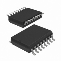
PCA9554AD,112 NXP Semiconductors, PCA9554AD,112 Datasheet - Page 25

PCA9554AD,112
Manufacturer Part Number
PCA9554AD,112
Description
IC I/O EXPANDER I2C 8B 16SOIC
Manufacturer
NXP Semiconductors
Datasheet
1.PCA9554ABS118.pdf
(30 pages)
Specifications of PCA9554AD,112
Package / Case
16-SOIC (0.300", 7.5mm Width)
Interface
I²C, SMBus
Number Of I /o
8
Interrupt Output
Yes
Frequency - Clock
400kHz
Voltage - Supply
2.3 V ~ 5.5 V
Operating Temperature
-40°C ~ 85°C
Mounting Type
Surface Mount
Includes
POR
Logic Family
PCA
Number Of Lines (input / Output)
8
Operating Supply Voltage
2.3 V to 5.5 V
Power Dissipation
200 mW
Operating Temperature Range
- 40 C to + 85 C
Maximum Clock Frequency
400 KHz
Mounting Style
SMD/SMT
Number Of Output Lines
8
Output Current
50 mA
Lead Free Status / RoHS Status
Lead free / RoHS Compliant
For Use With
OM6285 - EVAL BOARD I2C-2002-1A568-4002 - DEMO BOARD I2C
Lead Free Status / Rohs Status
Lead free / RoHS Compliant
Other names
568-1051-5
935269195112
PCA9554AD
935269195112
PCA9554AD
NXP Semiconductors
Table 13.
PCA9554_9554A_7
Product data sheet
Mounting
Through-hole mount
Through-hole-surface
mount
Suitability of IC packages for wave, reflow and dipping soldering methods
13.3.2 Wave soldering
13.3.3 Manual soldering
13.4 Package related soldering information
Conventional single wave soldering is not recommended for surface mount devices
(SMDs) or printed-circuit boards with a high component density, as solder bridging and
non-wetting can present major problems.
To overcome these problems the double-wave soldering method was specifically
developed.
If wave soldering is used the following conditions must be observed for optimal results:
During placement and before soldering, the package must be fixed with a droplet of
adhesive. The adhesive can be applied by screen printing, pin transfer or syringe
dispensing. The package can be soldered after the adhesive is cured.
Typical dwell time of the leads in the wave ranges from 3 seconds to 4 seconds at 250 C
or 265 C, depending on solder material applied, SnPb or Pb-free respectively.
A mildly-activated flux will eliminate the need for removal of corrosive residues in most
applications.
Fix the component by first soldering two diagonally-opposite end leads. Use a low voltage
(24 V or less) soldering iron applied to the flat part of the lead. Contact time must be
limited to 10 seconds at up to 300 C.
When using a dedicated tool, all other leads can be soldered in one operation within
2 seconds to 5 seconds between 270 C and 320 C.
Package
CPGA, HCPGA
DBS, DIP, HDIP, RDBS, SDIP, SIL
PMFP
•
•
•
Use a double-wave soldering method comprising a turbulent wave with high upward
pressure followed by a smooth laminar wave.
For packages with leads on two sides and a pitch (e):
– larger than or equal to 1.27 mm, the footprint longitudinal axis is preferred to be
– smaller than 1.27 mm, the footprint longitudinal axis must be parallel to the
The footprint must incorporate solder thieves at the downstream end.
For packages with leads on four sides, the footprint must be placed at a 45 angle to
the transport direction of the printed-circuit board. The footprint must incorporate
solder thieves downstream and at the side corners.
[4]
parallel to the transport direction of the printed-circuit board;
transport direction of the printed-circuit board.
[1]
Rev. 07 — 13 November 2006
Soldering method
Wave
suitable
suitable
not suitable
8-bit I
[3]
2
PCA9554/PCA9554A
C-bus and SMBus I/O port with interrupt
Reflow
not suitable
[2]
© NXP B.V. 2006. All rights reserved.
Dipping
suitable
25 of 30


