PCA9554AD,112 NXP Semiconductors, PCA9554AD,112 Datasheet - Page 6
PCA9554AD,112
Manufacturer Part Number
PCA9554AD,112
Description
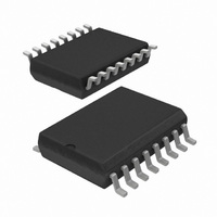
IC I/O EXPANDER I2C 8B 16SOIC
Manufacturer
NXP Semiconductors
Datasheet
1.PCA9554ABS118.pdf
(30 pages)
Specifications of PCA9554AD,112
Package / Case
16-SOIC (0.300", 7.5mm Width)
Interface
I²C, SMBus
Number Of I /o
8
Interrupt Output
Yes
Frequency - Clock
400kHz
Voltage - Supply
2.3 V ~ 5.5 V
Operating Temperature
-40°C ~ 85°C
Mounting Type
Surface Mount
Includes
POR
Logic Family
PCA
Number Of Lines (input / Output)
8
Operating Supply Voltage
2.3 V to 5.5 V
Power Dissipation
200 mW
Operating Temperature Range
- 40 C to + 85 C
Maximum Clock Frequency
400 KHz
Mounting Style
SMD/SMT
Number Of Output Lines
8
Output Current
50 mA
Lead Free Status / RoHS Status
Lead free / RoHS Compliant
For Use With
OM6285 - EVAL BOARD I2C-2002-1A568-4002 - DEMO BOARD I2C
Lead Free Status / Rohs Status
Lead free / RoHS Compliant
Other names
568-1051-5
935269195112
PCA9554AD
935269195112
PCA9554AD


NXP Semiconductors
6. Functional description
PCA9554_9554A_7
Product data sheet
6.1.1 Command byte
5.2 Pin description
6.1 Registers
Table 2.
[1]
Refer to
Table 3.
The command byte is the first byte to follow the address byte during a write transmission.
It is used as a pointer to determine which of the following registers will be written or read.
Symbol
A0
A1
A2
IO0
IO1
IO2
IO3
V
IO4
IO5
IO6
IO7
INT
SCL
SDA
V
n.c.
Command
0
1
2
3
SS
DD
HVQFN package die supply ground is connected to both V
connected to supply ground for proper device operation. For enhanced thermal, electrical, and board level
performance, the exposed pad needs to be soldered to the board using a corresponding thermal pad on the
board and for proper heat conduction through the board, thermal vias need to be incorporated in the PCB in
the thermal pad region.
Figure 1 “Block diagram of
Pin
DIP16, SO16,
SSOP16, TSSOP16
1
2
3
4
5
6
7
8
9
10
11
12
13
14
15
16
-
Pin description
Command byte
Protocol
read byte
read/write byte
read/write byte
read/write byte
Rev. 07 — 13 November 2006
HVQFN16 SSOP20
15
16
1
2
3
4
5
6
7
8
9
10
11
12
13
14
-
[1]
Function
Input Port register
Output Port register
Polarity Inversion register
Configuration register
PCA9554/PCA9554A”.
8-bit I
6
7
9
10
11
12
14
15
16
17
19
20
1
2
4
5
3, 8, 13, 18
2
PCA9554/PCA9554A
C-bus and SMBus I/O port with interrupt
SS
pin and exposed center pad. V
Description
address input 0
address input 1
address input 2
input/output 0
input/output 1
input/output 2
input/output 3
supply ground
input/output 4
input/output 5
input/output 6
input/output 7
interrupt output (open-drain)
serial clock line
serial data line
supply voltage
not connected
© NXP B.V. 2006. All rights reserved.
SS
pin must be
6 of 30
Related parts for PCA9554AD,112
Image
Part Number
Description
Manufacturer
Datasheet
Request
R

Part Number:
Description:
I/O Expanders, Repeaters & Hubs 8-BIT I2C FM TP GPIO
Manufacturer:
NXP Semiconductors
Datasheet:

Part Number:
Description:
NXP Semiconductors designed the LPC2420/2460 microcontroller around a 16-bit/32-bitARM7TDMI-S CPU core with real-time debug interfaces that include both JTAG andembedded trace
Manufacturer:
NXP Semiconductors
Datasheet:

Part Number:
Description:
NXP Semiconductors designed the LPC2458 microcontroller around a 16-bit/32-bitARM7TDMI-S CPU core with real-time debug interfaces that include both JTAG andembedded trace
Manufacturer:
NXP Semiconductors
Datasheet:
Part Number:
Description:
NXP Semiconductors designed the LPC2468 microcontroller around a 16-bit/32-bitARM7TDMI-S CPU core with real-time debug interfaces that include both JTAG andembedded trace
Manufacturer:
NXP Semiconductors
Datasheet:
Part Number:
Description:
NXP Semiconductors designed the LPC2470 microcontroller, powered by theARM7TDMI-S core, to be a highly integrated microcontroller for a wide range ofapplications that require advanced communications and high quality graphic displays
Manufacturer:
NXP Semiconductors
Datasheet:
Part Number:
Description:
NXP Semiconductors designed the LPC2478 microcontroller, powered by theARM7TDMI-S core, to be a highly integrated microcontroller for a wide range ofapplications that require advanced communications and high quality graphic displays
Manufacturer:
NXP Semiconductors
Datasheet:
Part Number:
Description:
The Philips Semiconductors XA (eXtended Architecture) family of 16-bit single-chip microcontrollers is powerful enough to easily handle the requirements of high performance embedded applications, yet inexpensive enough to compete in the market for hi
Manufacturer:
NXP Semiconductors
Datasheet:
Part Number:
Description:
The XA-S3 device is a member of Philips Semiconductors? XA(eXtended Architecture) family of high performance 16-bitsingle-chip microcontrollers
Manufacturer:
NXP Semiconductors
Datasheet:

Part Number:
Description:
The NXP BlueStreak LH75401/LH75411 family consists of two low-cost 16/32-bit System-on-Chip (SoC) devices
Manufacturer:
NXP Semiconductors
Datasheet:
Part Number:
Description:
The NXP LPC3130/3131 combine an 180 MHz ARM926EJ-S CPU core, high-speed USB2
Manufacturer:
NXP Semiconductors
Datasheet:
Part Number:
Description:
The NXP LPC3141 combine a 270 MHz ARM926EJ-S CPU core, High-speed USB 2
Manufacturer:
NXP Semiconductors
Part Number:
Description:
The NXP LPC3143 combine a 270 MHz ARM926EJ-S CPU core, High-speed USB 2
Manufacturer:
NXP Semiconductors

Part Number:
Description:
The NXP LPC3152 combines an 180 MHz ARM926EJ-S CPU core, High-speed USB 2
Manufacturer:
NXP Semiconductors
Part Number:
Description:
The NXP LPC3154 combines an 180 MHz ARM926EJ-S CPU core, High-speed USB 2
Manufacturer:
NXP Semiconductors