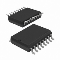
PCA9554AD,112 NXP Semiconductors, PCA9554AD,112 Datasheet - Page 9

PCA9554AD,112
Manufacturer Part Number
PCA9554AD,112
Description
IC I/O EXPANDER I2C 8B 16SOIC
Manufacturer
NXP Semiconductors
Datasheet
1.PCA9554ABS118.pdf
(30 pages)
Specifications of PCA9554AD,112
Package / Case
16-SOIC (0.300", 7.5mm Width)
Interface
I²C, SMBus
Number Of I /o
8
Interrupt Output
Yes
Frequency - Clock
400kHz
Voltage - Supply
2.3 V ~ 5.5 V
Operating Temperature
-40°C ~ 85°C
Mounting Type
Surface Mount
Includes
POR
Logic Family
PCA
Number Of Lines (input / Output)
8
Operating Supply Voltage
2.3 V to 5.5 V
Power Dissipation
200 mW
Operating Temperature Range
- 40 C to + 85 C
Maximum Clock Frequency
400 KHz
Mounting Style
SMD/SMT
Number Of Output Lines
8
Output Current
50 mA
Lead Free Status / RoHS Status
Lead free / RoHS Compliant
For Use With
OM6285 - EVAL BOARD I2C-2002-1A568-4002 - DEMO BOARD I2C
Lead Free Status / Rohs Status
Lead free / RoHS Compliant
Other names
568-1051-5
935269195112
PCA9554AD
935269195112
PCA9554AD
NXP Semiconductors
PCA9554_9554A_7
Product data sheet
Fig 9. Simplified schematic of IO0 to IO7
Remark: At power-on reset, all registers return to default values.
write configuration
write polarity
shift register
shift register
shift register
write pulse
read pulse
6.3 Interrupt output
6.4 I/O port
data from
data from
data from
pulse
pulse
The open-drain interrupt output is activated when one of the port pins change state and
the pin is configured as an input. The interrupt is deactivated when the input returns to its
previous state or the Input Port register is read.
Note that changing an I/O from and output to an input may cause a false interrupt to occur
if the state of the pin does not match the contents of the Input Port register.
When an I/O is configured as an input, FETs Q1 and Q2 are off, creating a
high-impedance input with a weak pull-up (100 k typ.) to V
raised above V
If the I/O is configured as an output, then either Q1 or Q2 is enabled, depending on the
state of the Output Port register. Care should be exercised if an external voltage is applied
to an I/O configured as an output because of the low-impedance paths that exist between
the pin and either V
configuration
register
D
CK
FF
Q
Q
DD
to a maximum of 5.5 V.
output port
register
D
CK
DD
Rev. 07 — 13 November 2006
FF
or V
Q
SS
.
input port
register
polarity inversion
register
D
CK
D
CK
FF
FF
Q
Q
8-bit I
2
PCA9554/PCA9554A
C-bus and SMBus I/O port with interrupt
Q1
Q2
100 k
DD
. The input voltage may be
output port
register data
V
IO0 to IO7
V
input port
register data
to INT
polarity inversion
register data
DD
SS
© NXP B.V. 2006. All rights reserved.
002aac493
9 of 30


