QLX4600LIQT7 Intersil, QLX4600LIQT7 Datasheet - Page 13
QLX4600LIQT7
Manufacturer Part Number
QLX4600LIQT7
Description
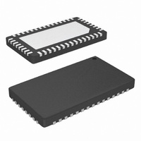
IC EQUALIZER REC 6.25GBPS 46QFN
Manufacturer
Intersil
Series
QLx™r
Specifications of QLX4600LIQT7
Applications
Data Transport
Voltage - Supply
1.1 V ~ 1.3 V
Package / Case
46-WQFN
Mounting Type
Surface Mount
Rohs Compliant
Yes
Lead Free Status / RoHS Status
Lead free / RoHS Compliant
Interface
-
Other names
QLX4600LIQT7-TR
Available stocks
Company
Part Number
Manufacturer
Quantity
Price
Company:

Part Number:
QLX4600LIQT7
Manufacturer:
Intersil
Quantity:
2 075


QLx4600-SL30 v3.0
APPLICATIONS INFORMATION
Several aspects of the QLx4600-SL30 are capable of being dynamically managed by a system controller to provide maximum flexibility and
optimum performance. These functions are controlled by interfacing to the highlighted pins in Figure 11. The specific procedures for
controlling these aspects of the QLx4600-SL30 are the focus of this section.
EQUALIZATION BOOST LEVEL
Channel equalization for the QLx4600-SL30 can be individually set to either (a) one of 18 levels through the DC voltages on external control
pins or (b) one of 32 levels via a set of registers programmed by a low speed serial bus. The pins used to control the boost level are
highlighted in Figure 11. Descriptions of these pins are listed in Table 7. Please refer to Table 6 for descriptions of all other pins on the
QLx4600-SL30.
DI
DO
CP3[A,B,C]
CP4[A,B,C]
MODE
CP2[C,B,A]
CP1[C,B,A]
ENB
CLK
Pin Name
FIGURE 11: PIN DIAGRAM HIGHLIGHTING PINS USED FOR DYNAMIC CONTROL OF THE QLx4600-SL30
16
17
18, 19, 20
21, 22, 23
39, 40, 41
42, 43, 44
45
46
Pin Number
24
TABLE 7: DESCRIPTIONS OF PINS USED TO SET EQUALIZATION BOOST LEVEL
Serial data input, CMOS logic. Input for serial data stream to program internal registers controlling the boost for
all four equalizers. Synchronized with clock (CLK) on pin 46. Overrides the boost setting established on CP
control pins. Internally pulled down.
Serial data output, CMOS logic. Output of the internal registers controlling the boost for all four equalizers.
Synchronized with clock on pin 46. Equivalent to serial data input on DI but delayed by 21 clock cycles.
Control pins for setting equalizer 3. CMOS logic inputs. Pins are read as a 3-digit number to set the boost level.
A is the MSB, and C is the LSB. Pins are internally pulled down through a 25kΩ resistor.
Control pins for setting equalizer 4. CMOS logic inputs. Pins are read as a 3-digit number to set the boost level.
A is the MSB, and C is the LSB. Pins are internally pulled down through a 25kΩ resistor.
Boost-level control mode input, CMOS logic. Allows serial programming of internal registers through pins DI,
ENB, and Clk when set HIGH. Resets all internal registers to zero and uses boost levels set by CP pins when
set LOW. If serial programming is not used, this pin should be grounded.
Control pins for setting equalizer 2. CMOS logic inputs. Pins are read as a 3-digit number to set the boost level.
A is the MSB, and C is the LSB. Pins are internally pulled down through a 25kΩ resistor.
Control pins for setting equalizer 1. CMOS logic inputs. Pins are read as a 3-digit number to set the boost level.
A is the MSB, and C is the LSB. Pins are internally pulled down through a 25kΩ resistor.
Serial data enable (active low), CMOS logic. Internal registers can be programmed with DI and CLK pins only
when the ENB pin is ‘LOW’. Internally pulled down.
Serial data clock, CMOS logic. Synchronous clock for serial data on DI and DO pins. Data on DI is latched on
the rising clock edge. Clock speed is recommended to be between 10MHz and 20MHz. Internally pulled down.
IN1[P]
IN1[N]
IN2[P]
IN2[N]
IN3[P]
IN3[N]
IN4[P]
IN4[N]
LOS1
LOS2
GND
V
V
V
DT
DD
DD
DD
10
11
12
13
14
15
1
2
3
4
5
6
7
8
9
46
16
45
17
QLx4600-SL30
44
18
46-Lead QFN
Exposed Pad
7mm x 4mm
0.4mm Pitch
Quellan
43
19
(GND)
13
42
20
41
21
40
22
39
23
38
37
36
35
34
33
32
31
30
29
28
27
26
25
24
Description
BGREF
OUT1[P]
OUT1[N]
V
OUT2[P]
OUT2[N]
V
OUT3[P]
OUT3[N]
V
OUT4[P]
OUT4[N]
LOS3
LOS4
MODE
DD
DD
DD
QLx4600-SL30
©2009 Quellan, Inc
Related parts for QLX4600LIQT7
Image
Part Number
Description
Manufacturer
Datasheet
Request
R

Part Number:
Description:
Quad Lane Extender
Manufacturer:
Intersil Corporation
Datasheet:
Part Number:
Description:
Quad Lane Extender
Manufacturer:
Intersil Corporation
Datasheet:
Part Number:
Description:
Intersil Corporation [CMOS Serial Controller Interface]
Manufacturer:
Intersil Corporation
Datasheet:
Part Number:
Description:
Manufacturer:
Intersil Corporation
Datasheet:
Part Number:
Description:
357-036-542-201 CARDEDGE 36POS DL .156 BLK LOPRO
Manufacturer:
Intersil Corporation
Datasheet:
Part Number:
Description:
1024-Word x 4-Bit LSI Static RAM
Manufacturer:
Intersil Corporation
Datasheet:
Part Number:
Description:
General Purpose NPN Transistor Arrays FN341.4
Manufacturer:
Intersil Corporation
Datasheet:
Part Number:
Description:
CMOS 16-Bit Microprocessor
Manufacturer:
Intersil Corporation
Datasheet:
Part Number:
Description:
Manufacturer:
Intersil Corporation
Datasheet:
Part Number:
Description:
Manufacturer:
Intersil Corporation
Datasheet:
Part Number:
Description:
Manufacturer:
Intersil Corporation
Datasheet:
Part Number:
Description:
Manufacturer:
Intersil Corporation
Datasheet:
Part Number:
Description:
CMOS 6-Bit Latch and Decoder Memory Interfaces
Manufacturer:
Intersil Corporation
Datasheet:
Part Number:
Description:
CA3046General Purpose NPN Transistor Arrays
Manufacturer:
Intersil Corporation
Datasheet:
Part Number:
Description:
Manufacturer:
Intersil Corporation
Datasheet: