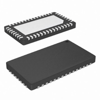
QLX4600LIQT7 Intersil, QLX4600LIQT7 Datasheet - Page 17

QLX4600LIQT7
Manufacturer Part Number
QLX4600LIQT7
Description
IC EQUALIZER REC 6.25GBPS 46QFN
Manufacturer
Intersil
Series
QLx™r
Specifications of QLX4600LIQT7
Applications
Data Transport
Voltage - Supply
1.1 V ~ 1.3 V
Package / Case
46-WQFN
Mounting Type
Surface Mount
Rohs Compliant
Yes
Lead Free Status / RoHS Status
Lead free / RoHS Compliant
Interface
-
Other names
QLX4600LIQT7-TR
Available stocks
Company
Part Number
Manufacturer
Quantity
Price
Company:
Part Number:
QLX4600LIQT7
Manufacturer:
Intersil
Quantity:
2 075
QLx4600-SL30 v3.0
SERIAL BUS PROGRAMMING
Pins 16 (DI), 45 (ENB), and 46 (CLK) are used to program the registers inside the QLx4600-SL30. Figure 12 shows an exemplary timing
diagram for the signals on these pins. The serial bus can be used to program a single QLx4600-SL30 according to the following steps:
PROGRAMMING MULTIPLE QLx4600-SL30 DEVICES
The serial bus interface provides a simple means of setting the equalizer boost levels with a minimal amount of board circuitry. Many of the
serial interface signals can be shared among the QLx4600-SL30 devices on a board and two options are presented in this section. The first
uses common clock and serial data signals along with separate ENB signals to select which QLx4600-SL30 accepts the programmed
changes. The second method uses a common ENB signal as the serial data is carried-over from one QLx4600-SL30 to the next.
1.
2.
3.
The ENB pin is pulled ‘LOW’.
At least 21 values are read from DI on the rising edge of the CLK signal.
The ENB pin is pulled ‘HIGH’ and the contents of the registers are latched and take effect.
FIGURE 12: TIMING DIAGRAM FOR PROGRAMMING THE INTERNAL REGISTERS OF THE QLx4600-SL30
While this pin is ‘LOW’, the data input on DI are read into registers but not yet latched.
A setup time of t
If more than 21 values are passed in, then only the last 21 values are kept in a FIFO fashion.
The data on DI should start by sending the value destined for register 21 and finish by sending the value destined for
register 1.
A range of clock frequencies can be used. A typical rate is 10MHz. The clock should not exceed 20MHz.
Setup (t
After clocking in the last data bit, an additional t
After completing these steps, the new values will affect within t
SDI
) and hold (t
SCK
is needed between ENB going ‘LOW’ and the first rising clock edge.
HDI
) times are needed around the rising clock edge.
17
HEN
should elapse before pulling the ENB signal ‘HIGH’.
D
.
QLx4600-SL30
©2009 Quellan, Inc


