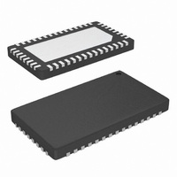
QLX4600LIQT7 Intersil, QLX4600LIQT7 Datasheet - Page 18

QLX4600LIQT7
Manufacturer Part Number
QLX4600LIQT7
Description
IC EQUALIZER REC 6.25GBPS 46QFN
Manufacturer
Intersil
Series
QLx™r
Specifications of QLX4600LIQT7
Applications
Data Transport
Voltage - Supply
1.1 V ~ 1.3 V
Package / Case
46-WQFN
Mounting Type
Surface Mount
Rohs Compliant
Yes
Lead Free Status / RoHS Status
Lead free / RoHS Compliant
Interface
-
Other names
QLX4600LIQT7-TR
Available stocks
Company
Part Number
Manufacturer
Quantity
Price
Company:
Part Number:
QLX4600LIQT7
Manufacturer:
Intersil
Quantity:
2 075
QLx4600-SL30
SEPARATE ENB SIGNALS
Multiple QLx4600-SL30 devices can be programmed from a common serial data stream as shown in Figure 13. Here, each QLx4600-SL30 is
provided its own ENB signal, and only one of these ENB signals is pulled ‘LOW’, and hence accepting the register data, at a time. In this
situation, the programming of each equalizer follows the steps outlined in Figure 14.
FIGURE 13: SERIAL BUS PROGRAMMING MULTIPLE QLx4600-SL30 DEVICES USING SEPARATE ENB SIGNALS
DI/DO CARRYOVER
The DO pin (pin 17) can be used to daisy-chain the serial bus among multiple QLx4600-SL30 chips. The DO pin outputs the overflow data
from the DI pin. Specifically, as data is pipelined into a QLx4600-SL30, it proceeds according to the following flow. First, a bit goes into
shadow register 1. Then, with each clock cycle, it shifts over into subsequent higher numbered registers. After shifting into register 21, it is
output on the DO pin on the same clock cycle. Thus, the DO signal is equal to the DI signal, but delayed by 20 clock cycles. The timing
diagram for the DO pin is shown in Figure 12 where the first 20 bits output from the DO are indefinite and subsequent bits are the data fed into
the DI pin. The delay between the rising clock edge and the data transition is t
.
CQ
FIGURE 14: TIMING DIAGRAM FOR DI/DO CARRYOVER
QLx4600-SL30 v3.0
18
©2009 Quellan, Inc


