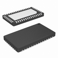
QLX4600LIQT7 Intersil, QLX4600LIQT7 Datasheet - Page 4

QLX4600LIQT7
Manufacturer Part Number
QLX4600LIQT7
Description
IC EQUALIZER REC 6.25GBPS 46QFN
Manufacturer
Intersil
Series
QLx™r
Specifications of QLX4600LIQT7
Applications
Data Transport
Voltage - Supply
1.1 V ~ 1.3 V
Package / Case
46-WQFN
Mounting Type
Surface Mount
Rohs Compliant
Yes
Lead Free Status / RoHS Status
Lead free / RoHS Compliant
Interface
-
Other names
QLX4600LIQT7-TR
Available stocks
Company
Part Number
Manufacturer
Quantity
Price
Company:
Part Number:
QLX4600LIQT7
Manufacturer:
Intersil
Quantity:
2 075
QLx4600-SL30 v3.0
Note 1: After channel loss, differential amplitudes at QLx4600-SL30 inputs must meet the input voltage range specified in Table 1.
Note 2: Temperature = 25ºC, V
Note 3: Output residual jitter is the difference between the total jitter at the lane extender output and the total jitter of the transmitted signal (as measured
Note 4: Measured using a PRBS 2
Note 5: Rise and fall times measured using a 1GHz clock with a 20ps edge rate.
Note 6: For active data mode, cable input amplitude is 400mVpp (differential) or greater. For line silence mode, cable input amplitude is 20mVpp
Note 7: Measured differentially across the data source.
Note 8: During line silence, transmitter noise in excess of this voltage range may result in differential output amplitudes from the QLx4600 that are greater
Note 9: The data pattern preceding line silence mode is comprised of the PCIe electrical idle ordered set (EIOS). The data pattern following line silence
Note 10: The data pattern preceding or following line silence mode is comprised of the SAS-2 ALIGN (0) sequence for OOB signaling at 3 Gb/s, and
SERIAL BUS TIMING CHARACTERISTICS
LOS De-Assert Time
Minimum Valid Transmitter
Amplitude
Maximum Allowable
Transmitter Output During
Line Silence
Data-to-Line Silence
Response Time
Line Silence-to-Data
Response Time
Timing Difference
CLK Setup Time
DI Setup Time
DI Hold Time
ENB ‘HIGH’
Boost Setting Operational
DO Hold Time
DO Valid
Clock Rate
at the input to the channel). Total jitter (TJ) is DJ
only.
(differential) or less.
than 20mVpp
mode is comprised of the PCIe electrical idle exit sequence (EIES).
amplitude of 800mVpp
Parameter
Parameter
DD
= 1.2V.
7
|t
-1 pattern. Deterministic jitter at the input to the lane extender is due to frequency-dependent, media-induced loss
Symbol
Symbol
DS
t
t
t
t
f
t
t
t
t
SCK
HEN
CLK
SDI
HDI
t
CQ
CV
- t
DS
SD
D
SD
|
From the falling edge of ENB
Prior to the rising edge of CLK
From the rising edge of CLK
From the falling edge of the last data bit’s CLK
From ENB ‘HIGH’
From the rising edge of CLK to DO transition
From the rising edge of CLK to DO valid
Reference clock for serial bus EQ programming
TABLE 5: SERIAL BUS TIMING CHARACTERISTICS
Time to de-assert Loss-of-Signal (LOS) indicator when
transitioning from line silence mode to active data mode
Active data transmission mode; 5Gb/s; Up to 20m 24AWG
standard twin-axial cable (approx.- 25dB loss at 2.5GHz);
DT current = 0μ
Line Silence mode; Up to 20m 24AWG standard twin-axial
cable (approx.- 25dB loss at 2.5GHz); DT current = 0μ
Time to transition from active data to line silence (muted
output) on 20m 24AWG standard twin-axial cable at 5Gb/s
Time from last bit of ALIGN(0) for SAS OOB signaling to
line silence (<20mVpp output); Meritec 24AWG 20m;
3Gb/s
Time to transition from line silence mode (muted output) to
active data on 20m 24AWG standard twin-axial cable at
5Gb/s
Time from first bit of ALIGN(0) for SAS OOB signaling to
450mVpp output; Meritec 24AWG 20m; 3Gb/s
For SAS OOB signaling support; Meritec 24AWG 20m
TABLE 4: ELECTRICAL CHARACTERISTICS
pp
+ 14.1 x RJ
A
Condition
RMS
.
Condition
4
Min
10
10
10
12
A
6
Min
500
Typ
Typ
Max
TBD
10
20
Max
100
20
15
14
20
19
Units
5
MHz
ns
ns
ns
ns
ns
ns
ns
QLx4600-SL30
mVpp
mVpp
Units
μs
ns
ns
ns
ns
ns
Notes
©2009 Quellan, Inc
Notes
6, 9
6, 9
7,8
10
10
10
6
7


