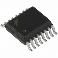
FSUSB22QSCX Fairchild Semiconductor, FSUSB22QSCX Datasheet - Page 3

FSUSB22QSCX
Manufacturer Part Number
FSUSB22QSCX
Description
IC USB SWITCH QUAD 2X1 16QSOP
Manufacturer
Fairchild Semiconductor
Type
Analog Switchr
Datasheet
1.FSUSB22BQX.pdf
(12 pages)
Specifications of FSUSB22QSCX
Function
USB Switch
Circuit
4 x 2:1
On-state Resistance
6.5 Ohm
Voltage Supply Source
Single Supply
Voltage - Supply, Single/dual (±)
3 V ~ 3.6 V
Current - Supply
1µA
Operating Temperature
-40°C ~ 85°C
Mounting Type
Surface Mount
Package / Case
16-QSOP
Multiplexer Configuration
Quad SPDT
Number Of Inputs
4
Number Of Outputs
8
Number Of Channels
4
Analog Switch On Resistance
7@3VOhm
Analog Switch Turn On Time
4.5ns
Analog Switch Turn Off Time
2.5ns
Package Type
QSOP W
Power Supply Requirement
Single
Single Supply Voltage (min)
3V
Single Supply Voltage (typ)
3V
Single Supply Voltage (max)
3.6V
Dual Supply Voltage (min)
Not RequiredV
Dual Supply Voltage (typ)
Not RequiredV
Dual Supply Voltage (max)
Not RequiredV
Power Dissipation
0.000001W
Mounting
Surface Mount
Pin Count
16
Operating Temp Range
-40C to 85C
Operating Temperature Classification
Industrial
Lead Free Status / RoHS Status
Lead free / RoHS Compliant
Other names
FSUSB22QSCXTR
FSUSB22QSCX_NL
FSUSB22QSCX_NLTR
FSUSB22QSCX_NLTR
FSUSB22QSCX_NL
FSUSB22QSCX_NLTR
FSUSB22QSCX_NLTR
© 2005 Fairchild Semiconductor Corporation
FSUSB22 • Rev. 1.0.3
Absolute Maximum Ratings
Stresses exceeding the absolute maximum ratings may damage the device. The device may not function or be
operable above the recommended operating conditions and stressing the parts to these levels is not recommended.
In addition, extended exposure to stresses above the recommended operating conditions may affect device
reliability. The absolute maximum ratings are stress ratings only.
Note:
1.
Recommended Operating Conditions
The Recommended Operating Conditions table defines the conditions for actual device operation. Recommended
operating conditions are specified to ensure optimal performance to the datasheet specifications. Fairchild does not
recommend exceeding them or designing to Absolute Maximum Ratings.
Note:
2.
Symbol
Symbol
I
CC
V
T
ESD
I
V
V
The input and output negative voltage ratings may be exceeded if the input and output diode current ratings are
observed.
t
Unused control inputs must be held HIGH or LOW. They may not float.
V
V
V
OUT
T
I
r
/ I
STG
OUT
, t
CC
IK
CC
IN
IN
S
A
GND
f
Supply Voltage
DC Switch Voltage
DC Input Voltage
DC Input Diode Current, V
DC Output Sink Current
DC V
Storage Temperature Range
Human Body Model, JESD22-A114
Power Supply Operating
Input Voltage
Output Voltage
Input Rise and Fall Time
Operating Temperature, Free Air
CC
/ GND Current
(1)
Parameter
Parameter
IN
<0V
Switch Control Input
Switch I/O
3
(2)
Min.
Min.
-0.5
-0.5
-0.5
-65
3.0
-40
0
0
0
0
V
CC
Max.
Max.
+150
±100
128
V
V
+85
DC
4.6
4.6
-50
3.6
+ 0.05
5
4
CC
CC
www.fairchildsemi.com
Unit
Unit
ns/V
mA
mA
mA
°C
kV
°C
V
V
V
V
V
V


