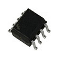
FM93C46EM8X Fairchild Semiconductor, FM93C46EM8X Datasheet

FM93C46EM8X
Specifications of FM93C46EM8X
Available stocks
Related parts for FM93C46EM8X
FM93C46EM8X Summary of contents
Page 1
... Microcontrollers and Microprocessors. There are 7 instructions implemented on the FM93C46 for various Read, Write, Erase, and Write Enable/Disable operations. This device is fabricated using Fairchild Semiconductor floating-gate CMOS process for high reliability, high endurance and low power consumption. “LZ” and “L” versions of FM93C46 offer very low standby current making them suitable for low power applications ...
Page 2
Pins designated as "NC" are typically unbonded pins. However some of them are bonded for special testing purposes. Hence if a signal is applied to these pins, care should be taken that ...
Page 3
Ambient Storage Temperature All Input or Output Voltages with Respect to Ground Lead Temperature (Soldering, 10 sec.) ESD rating I Operating Current CCA I Standby Current CCS I Input Leakage IL I Output Leakage OL V Input Low Voltage IL ...
Page 4
Ambient Storage Temperature All Input or Output Voltages with Respect to Ground Lead Temperature (Soldering, 10 sec.) ESD rating page 3 for V = 4.5V to 5.5V Operating Current CCA I Standby Current CCS L LZ (2.7V to ...
Page 5
... This is an active high input pin to FM93C46 EEPROM (the device) and is generated by a master that is controlling the device. A high level on this pin selects the device and a low level deselects the device. All serial communications with the device is enabled only when this pin is held high. However this pin cannot be permanently ...
Page 6
A typical Microwire cycle starts by first selecting the device (bringing the CS signal high). Once the device is selected, a valid Start bit (“1”) should be issued to properly recognize the cycle. Following this, the 2-bit opcode of appropriate ...
Page 7
... Refer Erase All cycle diagram. The Fairchild CMOS EEPROMs do not require an “ERASE” or “ERASE ALL” instruction prior to the “WRITE” or “WRITE ALL” instruction, respectively. The “ERASE” and “ERASE ALL” instructions are included to maintain compatibility with earlier technology EEPROMs ...
Page 8
SYNCHRONOUS DATA TIMING CS t CSS SK t DIS Valid Input DI DO (Data Read (Status Read) NORMAL READ CYCLE (READ Star t Opcode Bit Bits(2) DO 93C46: Address bits patter n ...
Page 9
WRITE DISABLE CYCLE (WDS ...
Page 10
ERASE CYCLE (ERASE ...
Page 11
All lead tips Typ. All Leads FM93C46 Rev. D.1 0.189 - 0.197 (4.800 ...
Page 12
Pin #1 IDENT 0.0433 Max (1.1) 0.0256 (0.65) Typ. Notes: Unless otherwise specified 1. Reference ...
Page 13
... Fairchild's products are not authorized for use as critical components in life support devices or systems without the express written approval of the President of Fairchild Semiconductor Corporation. As used herein: 1. Life support devices or systems are devices or systems which, (a) are intended for surgical implant into the body, or (b) support ...


