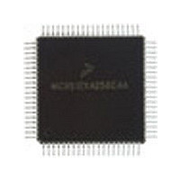
MC68HC912B32VFU8 Freescale Semiconductor, MC68HC912B32VFU8 Datasheet - Page 119

MC68HC912B32VFU8
Manufacturer Part Number
MC68HC912B32VFU8
Description
Manufacturer
Freescale Semiconductor
Datasheet
1.MC68HC912B32VFU8.pdf
(334 pages)
Specifications of MC68HC912B32VFU8
Cpu Family
HC12
Device Core Size
16b
Frequency (max)
8MHz
Interface Type
SCI/SPI
Program Memory Type
EPROM
Program Memory Size
32KB
Total Internal Ram Size
1KB
# I/os (max)
63
Operating Supply Voltage (typ)
5V
Operating Supply Voltage (max)
5.5V
Operating Supply Voltage (min)
4.5V
On-chip Adc
8-chx10-bit
Instruction Set Architecture
CISC
Operating Temp Range
-40C to 105C
Operating Temperature Classification
Industrial
Mounting
Surface Mount
Pin Count
80
Package Type
PQFP
Lead Free Status / Rohs Status
Not Compliant
Available stocks
Company
Part Number
Manufacturer
Quantity
Price
Part Number:
MC68HC912B32VFU8
Manufacturer:
MOTOROLA/摩托罗拉
Quantity:
20 000
- Current page: 119 of 334
- Download datasheet (2Mb)
10.7.3 Real-Time Interrupt Flag Register
RTIF — Real-Time Interrupt Flag Bit
10.7.4 COP Control Register
Read: Anytime
Write: Varies on a bit by bit basis
CME — Clock Monitor Enable Bit
FCME — Force Clock Monitor Enable Bit
FCM — Force Clock Monitor Reset Bit
Freescale Semiconductor
This bit is cleared automatically by a write to this register with this bit set.
Write anytime.
If FCME is set, this bit has no meaning or effect.
Write once in normal modes, anytime in special modes.
In normal modes, when this bit is set, the clock monitor function cannot be disabled until a reset occurs.
To use both STOP and clock monitor, the CME bit should be cleared prior to executing a STOP
instruction and set after recovery from STOP. Always keep FCME = 0, if STOP will be used.
Writes are not allowed in normal modes, anytime in special modes.
If DISR is set, this bit has no effect.
0 = Timeout has not yet occurred.
1 = Set when the timeout period is met
0 = Clock monitor is disabled; slow clocks and STOP instruction may be used.
1 = Slow or stopped clocks (including the STOP instruction) cause a clock reset sequence.
0 = Clock monitor follows the state of the CME bit.
1 = Slow or stopped clocks cause a clock reset sequence.
0 = Normal operation
1 = Force a clock monitor reset, if clock monitor is enabled.
Normal Reset:
Special Reset:
Address: $0015
Address: $0016
Reset:
Read:
Write:
Read:
Write:
Figure 10-7. Real-Time Interrupt Flag Register (RTIFLG)
RTIF
Bit 7
CME
0
Bit 7
0
0
Figure 10-8. COP Control Register (COPCTL)
FCME
6
0
0
6
0
0
M68HC12B Family Data Sheet, Rev. 9.1
5
0
0
FCM
5
0
0
FCOP
4
0
0
4
0
0
DISR
3
0
0
3
0
1
2
0
0
CR2
2
0
0
1
0
0
CR1
1
0
0
Bit 0
0
0
Bit 0
CR0
1
1
Clock Registers
119
Related parts for MC68HC912B32VFU8
Image
Part Number
Description
Manufacturer
Datasheet
Request
R
Part Number:
Description:
Manufacturer:
Freescale Semiconductor, Inc
Datasheet:
Part Number:
Description:
Manufacturer:
Freescale Semiconductor, Inc
Datasheet:
Part Number:
Description:
Manufacturer:
Freescale Semiconductor, Inc
Datasheet:
Part Number:
Description:
Manufacturer:
Freescale Semiconductor, Inc
Datasheet:
Part Number:
Description:
Manufacturer:
Freescale Semiconductor, Inc
Datasheet:
Part Number:
Description:
Manufacturer:
Freescale Semiconductor, Inc
Datasheet:
Part Number:
Description:
Manufacturer:
Freescale Semiconductor, Inc
Datasheet:
Part Number:
Description:
Manufacturer:
Freescale Semiconductor, Inc
Datasheet:
Part Number:
Description:
Manufacturer:
Freescale Semiconductor, Inc
Datasheet:
Part Number:
Description:
Manufacturer:
Freescale Semiconductor, Inc
Datasheet:
Part Number:
Description:
Manufacturer:
Freescale Semiconductor, Inc
Datasheet:
Part Number:
Description:
Manufacturer:
Freescale Semiconductor, Inc
Datasheet:
Part Number:
Description:
Manufacturer:
Freescale Semiconductor, Inc
Datasheet:
Part Number:
Description:
Manufacturer:
Freescale Semiconductor, Inc
Datasheet:
Part Number:
Description:
Manufacturer:
Freescale Semiconductor, Inc
Datasheet:


