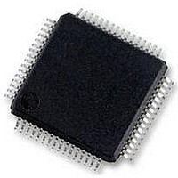
STM32F405RGT6 STMicroelectronics, STM32F405RGT6 Datasheet - Page 119

STM32F405RGT6
Manufacturer Part Number
STM32F405RGT6
Description
Microcontrollers (MCU) ARM M4 1024 FLASH 168 Mhz 192kB SRAM
Manufacturer
STMicroelectronics
Datasheet
1.STM32F407ZGT6.pdf
(167 pages)
Specifications of STM32F405RGT6
Core
ARM Cortex M4
Processor Series
STM32F4
Data Bus Width
32 bit
Maximum Clock Frequency
168 MHz
Program Memory Size
1024 KB
Data Ram Size
192 KB
On-chip Adc
Yes
Number Of Programmable I/os
51
Number Of Timers
10
Operating Supply Voltage
1.7 V to 3.6 V
Package / Case
LQFP-64
Mounting Style
SMD/SMT
A/d Bit Size
12 bit
A/d Channels Available
16
Interface Type
CAN, I2C, I2S, SPI, UART
Program Memory Type
Flash
Lead Free Status / Rohs Status
Details
Available stocks
Company
Part Number
Manufacturer
Quantity
Price
Company:
Part Number:
STM32F405RGT6
Manufacturer:
ON
Quantity:
1 001
Company:
Part Number:
STM32F405RGT6
Manufacturer:
STMicroelectronics
Quantity:
10 000
Part Number:
STM32F405RGT6
Manufacturer:
ST
Quantity:
20 000
STM32F405xx, STM32F407xx
Table 65.
1. TBD stands for “to be defined”.
2. If an inverted reset signal is applied to PDR_ON, this value can be lowered to 1.7 V when the device operates in a reduced
3. It is recommended to maintain the voltage difference between V
4. V
5. Based on characterization, not tested in production.
6. V
7. R
8. For external triggers, a delay of 1/f
I
I
VREF+
DDA
Symbol
t
t
CONV
STAB
temperature range (0 to 70 °C).
t
f
S
S
DDA
REF+
ADC
(5)
(5)
(5)
(5)
(5)
(5)
-V
maximum value is given for V
is internally connected to V
REF+
Sampling time
Power-up time
Total conversion time (including
sampling time)
Sampling rate
(f
t
ADC V
consumption in conversion
mode
ADC V
consumption in conversion
mode
S
ADC
ADC characteristics
= 3 ADC cycles)
< 1.2 V.
= 30 MHz, and
REF
DDA
Parameter
DC current
DC current
DDA
PCLK2
DD
=1.8 V, and minimum value for V
and V
(1)
must be added to the latency specified in
(continued)
REF-
9 to 492 (t
approximation)
Interleave Triple ADC
Interleave Dual ADC
is internally connected to V
Doc ID 022152 Rev 2
480 sampling time
480 sampling time
12-bit resolution
10-bit resolution
12-bit resolution
12-bit resolution
12-bit resolution
12-bit resolution
12-bit resolution
12-bit resolution
12-bit resolution
3 sampling time
3 sampling time
f
f
f
f
8-bit resolution
f
6-bit resolution
f
f
f
f
ADC
ADC
ADC
ADC
ADC
ADC
ADC
ADC
ADC
Single ADC
Conditions
mode
mode
= 30 MHz
= 30 MHz
= 30 MHz
= 30 MHz
= 30 MHz
= 30 MHz
= 30 MHz
= 30 MHz
= 30 MHz
S
for sampling +n-bit resolution for successive
REF+
and V
DD
=3.3 V.
DDA
SSA
below 1.8 V.
.
0.100
0.416
0.360
0.305
0.250
Min
Table
3
-
-
-
-
-
-
-
-
65.
Electrical characteristics
Typ
300
1.6
2
-
-
-
-
-
-
-
-
-
-
-
12.95
12.89
12.84
12.79
TBD
TBD
Max
3.75
416
500
1.8
16
3
2
6
119/167
1/f
1/f
Msps
Msps
Msps
Unit
mA
µA
µA
µs
µs
µs
µs
µs
µs
ADC
ADC


