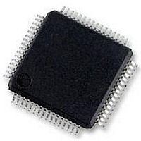
STM32F405RGT6 STMicroelectronics, STM32F405RGT6 Datasheet - Page 120

STM32F405RGT6
Manufacturer Part Number
STM32F405RGT6
Description
Microcontrollers (MCU) ARM M4 1024 FLASH 168 Mhz 192kB SRAM
Manufacturer
STMicroelectronics
Datasheet
1.STM32F407ZGT6.pdf
(167 pages)
Specifications of STM32F405RGT6
Core
ARM Cortex M4
Processor Series
STM32F4
Data Bus Width
32 bit
Maximum Clock Frequency
168 MHz
Program Memory Size
1024 KB
Data Ram Size
192 KB
On-chip Adc
Yes
Number Of Programmable I/os
51
Number Of Timers
10
Operating Supply Voltage
1.7 V to 3.6 V
Package / Case
LQFP-64
Mounting Style
SMD/SMT
A/d Bit Size
12 bit
A/d Channels Available
16
Interface Type
CAN, I2C, I2S, SPI, UART
Program Memory Type
Flash
Lead Free Status / Rohs Status
Details
Available stocks
Company
Part Number
Manufacturer
Quantity
Price
Company:
Part Number:
STM32F405RGT6
Manufacturer:
ON
Quantity:
1 001
Company:
Part Number:
STM32F405RGT6
Manufacturer:
STMicroelectronics
Quantity:
10 000
Part Number:
STM32F405RGT6
Manufacturer:
ST
Quantity:
20 000
Electrical characteristics
Note:
120/167
Equation 1: R
The formula above
allowed for an error below 1/4 of LSB. N = 12 (from 12-bit resolution) and k is the number of
sampling periods defined in the ADC_SMPR1 register.
Table 66.
1. Better performance could be achieved in restricted V
2. Based on characterization, not tested in production.
3. If an inverted reset signal is applied to PDR_ON, this value can be lowered to 1.7 V when the device
ADC accuracy vs. negative injection current: Injecting a negative current on any of the
standard (non-robust) analog input pins should be avoided as this significantly reduces the
accuracy of the conversion being performed on another analog input. It is recommended to
add a Schottky diode (pin to ground) to standard analog pins which may potentially inject
negative currents.
Any positive injection current within the limits specified for I
Section 5.3.16
Symbol
a
operates in a reduced temperature range (0 to 70 °C).
EO
EG
ED
ET
EL
Total unadjusted error
Offset error
Gain error
Differential linearity error
Integral linearity error
ADC accuracy at f
AIN
does not affect the ADC accuracy.
Parameter
max formula
(Equation
R
AIN
1) is used to determine the maximum external impedance
Doc ID 022152 Rev 2
=
ADC
------------------------------------------------------------- - R
f
ADC
= 30 MHz
f
f
V
PCLK2
ADC
DDA
×
C
(
= 30 MHz, R
k 0.5
= 1.8
ADC
= 60 MHz,
Test conditions
–
DD
(1)
×
(3)
, frequency and temperature ranges.
ln
to 3.6 V
)
(
2
N
AIN
+
2
< 10 kΩ,
)
–
INJ(PIN)
STM32F405xx, STM32F407xx
ADC
and ΣI
±1.5
±1.5
±1.5
Typ
±2
±1
INJ(PIN)
Max
±2.5
±3
±2
±5
±3
(2)
in
Unit
LSB


