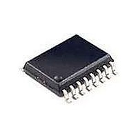
SI3050-KT Silicon Laboratories Inc, SI3050-KT Datasheet - Page 13

SI3050-KT
Manufacturer Part Number
SI3050-KT
Description
IC VOICE DAA GCI/PCM/SPI 20TSSOP
Manufacturer
Silicon Laboratories Inc
Type
Chipsetr
Specifications of SI3050-KT
Package / Case
20-TSSOP
Function
Data Access Arrangement (DAA)
Interface
PCM, Serial, SPI
Number Of Circuits
1
Voltage - Supply
3 V ~ 3.6 V
Current - Supply
8.5mA
Operating Temperature
0°C ~ 70°C
Mounting Type
Surface Mount
Includes
Line Voltage Monitor, Loop Current Monitor, Overload Detection, Parallel Handset Detection, Polarity Reversal Detection, TIP and
Product
Modem Chip
Supply Voltage (min)
3 V
Supply Current
8.5 mA
Maximum Operating Temperature
+ 70 C
Minimum Operating Temperature
0 C
Mounting Style
SMD/SMT
Lead Free Status / RoHS Status
Contains lead / RoHS non-compliant
Power (watts)
-
Lead Free Status / RoHS Status
Lead free / RoHS Compliant, Contains lead / RoHS non-compliant
Available stocks
Company
Part Number
Manufacturer
Quantity
Price
Part Number:
SI3050-KT
Manufacturer:
SILICONIX
Quantity:
20 000
Company:
Part Number:
SI3050-KTR
Manufacturer:
NEC
Quantity:
947
Part Number:
SI3050-KTR
Manufacturer:
SILICON LABS/芯科
Quantity:
20 000
Table 9. Switching Characteristics—GCI Highway Serial Interface
(V
Parameter
Cycle Time PCLK (Single Clocking Mode)
Cycle Time PCLK (Double Clocking Mode)
Valid PCLK Inputs
FSYNC Period
PCLK Duty Cycle
FSYNC Jitter Tolerance
Rise Time, PCLK
Fall Time, PCLK
Delay Time, PCLK Rise to DTX Active
Delay Time, PCLK Rise to DTX Transition
Delay Time, PCLK Rise to DTX Tri-State
Setup Time, FSYNC Rise to PCLK Fall
Hold Time, PCLK Fall to FSYNC Fall
Setup Time, DRX Transition to PCLK Fall
Hold Time, PCLK Falling to DRX Transition
Notes:
D
=
1. All timing is referenced to the 50% level of the waveform. Input test levels are V
2. FSYNC must be 8 kHz under all operating conditions.
3. Specification applies to PCLK fall to DTX tri-state when that mode is selected.
3.0 to 3.6 V, T
times are referenced to the 20% and 80% levels of the waveform.
1
FSYNC
2
DRX
PCLK
DTX
A
Figure 5. GCI Highway Interface Timing Diagram (1x PCLK Mode)
=
0 to 70 °C for K-Grade, C
t
d1
t
su1
t
h1
3
L
=
Symbol
20 pF)
t
t
t
t
jitter
t
t
t
t
t
su1
su2
t
t
t
dty
d1
d2
d3
h1
h2
t
t
fp
p
p
r
f
Rev. 1.0
t
su2
t
d2
t
p
Conditions
t
Test
h2
t
fp
t
r
Min
40
25
20
25
20
—
—
—
—
—
—
—
—
—
—
—
IH
=
V
O
– 0.4 V, V
2.048
4.096
Typ
488
244
125
50
—
—
—
—
—
—
—
—
—
—
t
f
t
d3
IL
=
0.4 V, rise and fall
±120
Max
Si3050
60
25
25
20
20
20
—
—
—
—
—
—
—
—
—
Units
MHz
MHz
ns
ns
ns
ns
ns
ns
ns
ns
ns
ns
ns
ns
ns
%
13


