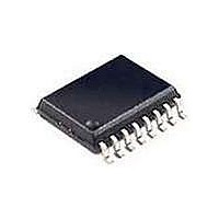
SI3050-KT Silicon Laboratories Inc, SI3050-KT Datasheet - Page 23

SI3050-KT
Manufacturer Part Number
SI3050-KT
Description
IC VOICE DAA GCI/PCM/SPI 20TSSOP
Manufacturer
Silicon Laboratories Inc
Type
Chipsetr
Specifications of SI3050-KT
Package / Case
20-TSSOP
Function
Data Access Arrangement (DAA)
Interface
PCM, Serial, SPI
Number Of Circuits
1
Voltage - Supply
3 V ~ 3.6 V
Current - Supply
8.5mA
Operating Temperature
0°C ~ 70°C
Mounting Type
Surface Mount
Includes
Line Voltage Monitor, Loop Current Monitor, Overload Detection, Parallel Handset Detection, Polarity Reversal Detection, TIP and
Product
Modem Chip
Supply Voltage (min)
3 V
Supply Current
8.5 mA
Maximum Operating Temperature
+ 70 C
Minimum Operating Temperature
0 C
Mounting Style
SMD/SMT
Lead Free Status / RoHS Status
Contains lead / RoHS non-compliant
Power (watts)
-
Lead Free Status / RoHS Status
Lead free / RoHS Compliant, Contains lead / RoHS non-compliant
Available stocks
Company
Part Number
Manufacturer
Quantity
Price
Part Number:
SI3050-KT
Manufacturer:
SILICONIX
Quantity:
20 000
Company:
Part Number:
SI3050-KTR
Manufacturer:
NEC
Quantity:
947
Part Number:
SI3050-KTR
Manufacturer:
SILICON LABS/芯科
Quantity:
20 000
Power Supplies
The Si3050 operates from a 3.0–3.6 V power supply.
The Si3050 input pins can only accept 3.3 V CMOS
signal levels. If support of 5 V signal levels is necessary,
a level shifter is required. The Si3018/19 derives its
power from two sources: the Si3050 and the telephone
line. The Si3050 supplies power over the patented
ISOcap link between the two devices, allowing the
Si3019 to communicate with the Si3050 while on-hook
and perform other on-hook functions, such as line
voltage monitoring. When off-hook, the Si3018/19 also
derives power from the line current supplied from the
telephone line. This feature is exclusive to DAAs from
Silicon Labs and allows the most cost-effective
implementation for a DAA while still maintaining robust
performance over all line conditions.
Initialization
Each time the Si3050 is powered up, assert the RESET
pin. When the RESET pin is deasserted, the registers
have default values to guarantee the line-side device
(Si3018/19) is powered down without the possibility of
loading the line (i.e., off-hook). An example initialization
procedure follows:
1. Supply the appropriate PCLK and FSYNC signals to the
2. Wait until the PLL is locked. This time is less than 1 m
3. Write an 00H into Register 6 to power up the line-side
4. Set the desired line interface parameters (i.e., DCV[1:0],
When this procedure is complete, the Si3018/19 is
ready for ring detection and off-hook operation.
Isolation Barrier
The Si3050 achieves an isolation barrier through
low-cost, high-voltage capacitors in conjunction with
Silicon
processing
eliminates
mismatches, common mode interference, or noise
coupling.
Schematic" on page 17, the C1, C2, C8, and C9
capacitors isolate the Si3050 (system-side) from the
Si3018/19 (line-side). Transmit, receive, control, ring
detect, and caller ID data are passed across this barrier.
The ISOcap communications link is disabled by default.
To enable it, the PDL bit (Register 6, bit 4) must be
cleared. No communication between the Si3050 and
Si3018/19 can occur until this bit is cleared. Allow the
Si3050.
from the application of PCLK.
device (Si3018/19).
MINI[1:0], ILIM, DCR, ACIM[3:0], OHS, RT, RZ, TGA2, and
TXG2[3:0]) shown in Table 13 on page 21.
Laboratories’
As
techniques.
signal
shown
degradation
in
proprietary
ISOcap
the
"Typical
signal
from
ISOcap
Application
processing
capacitor
signal
s
Rev. 1.0
PLL to lock to the PCLK and FSYNC input signals
before clearing the PDL bit.
Power Management
The Si3050 supports four basic power management
operation modes. The modes are normal operation,
reset operation, sleep mode, and full powerdown mode.
The power management modes are controlled by the
PDN and PDL bits (Register 6).
On powerup, or following a reset, the Si3050 is in reset
operation. The PDL bit is set, and the PDN bit is
cleared. The Si3050 is operational, except for the
ISOcap link. No communication between the Si3050
and line-side device (Si3018/19) can occur during reset
operation. Bits associated with the line-side device are
invalid in this mode.
The most common mode of operation is the normal
operation. The PDL and PDN bits are cleared. The DAA
is operational and the ISOcap link passes information
between the Si3050 and the Si3018 or Si3019.
The Si3050 supports a low-power sleep mode that
supports ring validation and wake-up-on-ring features.
To enable the sleep mode, the PDN bit must be set.
When the Si3050 is in sleep mode, the PCLK signal
must remain active. In low-power sleep mode, the
Si3050 is non-functional except for the ISOcap link and
the RGDT signal. To take the Si3050 out of sleep mode,
pulse the reset pin (RESET) low.
In summary, the powerdown/up sequence for sleep
mode is as follows:
1. Ensure the PDL bit (Register 6, bit 4) is cleared.
2. Set the PDN bit (Register 6
3. PCLK must remain active.
4. Reset the Si3050 by pulsing the RESET pin.
5. Program registers to desired settings.
The Si3050 also supports an additional Powerdown
mode. When both the PDN (Register 6, bit 3) and PDL
(Register 6, bit 4) bits are set, the chipset enters a
complete powerdown mode and draws negligible
current (deep sleep mode). In this mode, the Si3050 is
non-functional. The RGDT pin does not function and the
Si3050 will not detect a ring. Normal operation can be
restored using the same process for taking the Si3050
out of sleep mode.
Calibration
The Si3050 initiates two auto-calibrations by default
when the device goes off-hook or experiences a loss of
line power. A 17 ms resistor calibration is performed to
allow circuitry internal to the DAA to adjust to the exact
line conditions present at the time of going off-hook.
This resistor calibration can be disabled by setting the
, bit
3).
Si3050
23


