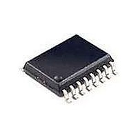
SI3050-KT Silicon Laboratories Inc, SI3050-KT Datasheet - Page 8

SI3050-KT
Manufacturer Part Number
SI3050-KT
Description
IC VOICE DAA GCI/PCM/SPI 20TSSOP
Manufacturer
Silicon Laboratories Inc
Type
Chipsetr
Specifications of SI3050-KT
Package / Case
20-TSSOP
Function
Data Access Arrangement (DAA)
Interface
PCM, Serial, SPI
Number Of Circuits
1
Voltage - Supply
3 V ~ 3.6 V
Current - Supply
8.5mA
Operating Temperature
0°C ~ 70°C
Mounting Type
Surface Mount
Includes
Line Voltage Monitor, Loop Current Monitor, Overload Detection, Parallel Handset Detection, Polarity Reversal Detection, TIP and
Product
Modem Chip
Supply Voltage (min)
3 V
Supply Current
8.5 mA
Maximum Operating Temperature
+ 70 C
Minimum Operating Temperature
0 C
Mounting Style
SMD/SMT
Lead Free Status / RoHS Status
Contains lead / RoHS non-compliant
Power (watts)
-
Lead Free Status / RoHS Status
Lead free / RoHS Compliant, Contains lead / RoHS non-compliant
Available stocks
Company
Part Number
Manufacturer
Quantity
Price
Part Number:
SI3050-KT
Manufacturer:
SILICONIX
Quantity:
20 000
Company:
Part Number:
SI3050-KTR
Manufacturer:
NEC
Quantity:
947
Part Number:
SI3050-KTR
Manufacturer:
SILICON LABS/芯科
Quantity:
20 000
Table 4. AC Characteristics
(V
Si3050
8
Sample Rate
PCLK Input Frequency
Receive Frequency Response
Receive Frequency Response
Transmit Full Scale Level
Receive Full Scale Level
Dynamic Range
Dynamic Range
Dynamic Range
Transmit Total Harmonic
Distortion
Transmit Total Harmonic
Distortion
Receive Total Harmonic
Distortion
Receive Total Harmonic
Distortion
Dynamic Range (Caller ID mode)
Caller ID Full Scale Level
Gain Accuracy
Notes:
Parameter
D
=
1. Measured at TIP and RING with 600 Ω termination at 1 kHz, as shown in Figure 1 on page 6.
2. The transmit and receive full scale level of +3.2 dBm can be achieved with a 600 Ω ac termination. While the transmit
3. Receive full scale level produces –0.9 dBFS at DTX.
4. DR
5. Measurement is 300 to 3400 Hz. Applies to both transmit and receive paths.
6. Vin
7. THD
8. DR
9. Refer to Tables 10–11 for relative gain accuracy characteristics (passband ripple).
3.0 to 3.6 V, T
and receive level in dBm varies with reference impedance, the DAA will transmit and receive 1 dBV into all reference
impedances.
above.
CID
6,7
6,7
6,7
6,7
=
=
=
1 kHz, –3 dBFS.
20 x log (rms V
=
20 x log (rms distortion/rms signal).
6,9
20 x log (rms V
4,5,6
4,5,6
4,5,6
A
=
0 to 70 °C for K-Grade,
1,3
1
8
FS
/rms Vin) + 20 x log (rms V
CID
/rms V
8
Symbol
IN
DR
PCLK
THD
THD
THD
THD
V
) + 20 x log (rms V
V
V
DR
DR
DR
Fs
CID
FS
FS
CID
Fs = 8000 Hz,
Low –3 dBFS Corner, FILT = 0
Low –3 dBFS Corner, FILT = 1
ILIM = 0, DCV = 11, MINI=00
ILIM = 0, DCV = 00, MINI=11
ILIM = 1, DCV = 11, MINI=00
ILIM = 0, DCV = 11, MINI=00
ILIM = 0, DCV = 00, MINI=11
ILIM = 0, DCV = 00, MINI=11
ILIM = 1,DCV = 11, MINI=00
VIN = 1 kHz, –13 dBFS
FULL = 1 (+3.2 dBm)
FULL = 1 (+3.2 dBm)
in
DCR = 0, I
DCR = 0, I
TXG2, RXG2, TXG3,
DCR = 0, I
DCR = 0, I
DCR = 0, I
DCR = 0, I
DCR = 0, I
/rms noise). Here, V
Rev. 1.0
FULL = 0 (0 dBm)
FULL = 0 (0 dBm)
and RXG3 = 0000
Test Condition
IN
2-W to DTX,
/rms noise). V
see
"Typical Application Schematic" on page 17
L
L
L
L
L
L
L
= 100 mA
= 100 mA
= 20 mA
= 50 mA
= 20 mA
= 20 mA
= 50 mA
CID
FS
is the 1.5 V full-scale level.
2
2
is the 0 dBm full-scale level per Note 1
–0.5
Min
256
—
—
—
—
—
—
—
—
—
—
—
—
—
—
—
8
1.52
1.52
Typ
200
–72
–78
–78
–78
1.1
1.1
1.5
80
80
80
62
—
—
5
0
8192
Max
0.5
16
—
—
—
—
—
—
—
—
—
—
—
—
—
—
—
)
V
V
V
V
V
Unit
kHz
kHz
PEAK
PEAK
PEAK
PEAK
PEAK
Hz
Hz
dB
dB
dB
dB
dB
dB
dB
dB
dB


