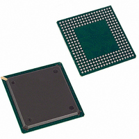
DS21Q55 Maxim Integrated Products, DS21Q55 Datasheet - Page 130

DS21Q55
Manufacturer Part Number
DS21Q55
Description
IC TXRX QUAD T1/E1/J1 SCT 256BGA
Manufacturer
Maxim Integrated Products
Datasheet
1.DS21Q55.pdf
(237 pages)
Specifications of DS21Q55
Function
Transceiver
Interface
E1, J1, T1
Number Of Circuits
4
Voltage - Supply
3.14 V ~ 3.47 V
Current - Supply
75mA
Operating Temperature
0°C ~ 70°C
Mounting Type
Surface Mount
Package / Case
256-BGA
Includes
BERT Generator and Detector, Dual HDLC Controllers
Lead Free Status / RoHS Status
Contains lead / RoHS non-compliant
Power (watts)
-
Available stocks
Company
Part Number
Manufacturer
Quantity
Price
Company:
Part Number:
DS21Q552
Manufacturer:
DALLAS
Quantity:
319
Company:
Part Number:
DS21Q552BN+
Manufacturer:
Maxim Integrated
Quantity:
10 000
Part Number:
DS21Q554
Manufacturer:
DALLAS
Quantity:
20 000
Part Number:
DS21Q554B+
Manufacturer:
MAXIM/美信
Quantity:
20 000
DS21Q55 Quad T1/E1/J1 Transceiver
21.
HDLC CONTROLLERS
This device has two enhanced HDLC controllers, HDLC #1 and HDLC #2. Each controller is
configurable for use with time slots, Sa4 to Sa8 bits (E1 mode), or the FDL (T1 mode). Each HDLC
controller has 128-byte buffers in the transmit and receive paths. When used with time slots, the user can
select any time slot or multiple time slots, contiguous or noncontiguous, as well as any specific bits
within the time slot(s) to assign to the HDLC controllers.
The user must not map both transmit HDLC controllers to the same Sa bits, time slots or, in T1 mode,
map both controllers to the FDL. HDLC #1 and HDLC #2 are identical in operation and therefore the
following operational description refers only to a singular controller.
The HDLC controller performs the entire necessary overhead for generating and receiving performance
report messages (PRMs) as described in ANSI T1.403 and the messages as described in AT&T TR54016.
The HDLC controller automatically generates and detects flags, generates and checks the CRC check
sum, generates and detects abort sequences, stuffs and destuffs zeros, and byte aligns to the data stream.
The 128-byte buffers in the HDLC controller are large enough to allow a full PRM to be received or
transmitted without host intervention.
21.1 Basic Operation Details
The HDLC registers are divided into four groups: control/configuration, status/information, mapping, and
FIFOs.
Table 21-A
lists these registers by group.
21.2 HDLC Configuration
The HxTC and HxRC registers perform the basic configuration of the HDLC controllers. Operating
features such as CRC generation, zero stuffer, transmit and receive HDLC mapping options, and idle
flags are selected here. These registers also reset the HDLC controllers.
130 of 237


