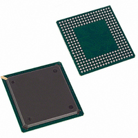
DS21Q55 Maxim Integrated Products, DS21Q55 Datasheet - Page 147

DS21Q55
Manufacturer Part Number
DS21Q55
Description
IC TXRX QUAD T1/E1/J1 SCT 256BGA
Manufacturer
Maxim Integrated Products
Datasheet
1.DS21Q55.pdf
(237 pages)
Specifications of DS21Q55
Function
Transceiver
Interface
E1, J1, T1
Number Of Circuits
4
Voltage - Supply
3.14 V ~ 3.47 V
Current - Supply
75mA
Operating Temperature
0°C ~ 70°C
Mounting Type
Surface Mount
Package / Case
256-BGA
Includes
BERT Generator and Detector, Dual HDLC Controllers
Lead Free Status / RoHS Status
Contains lead / RoHS non-compliant
Power (watts)
-
Available stocks
Company
Part Number
Manufacturer
Quantity
Price
Company:
Part Number:
DS21Q552
Manufacturer:
DALLAS
Quantity:
319
Company:
Part Number:
DS21Q552BN+
Manufacturer:
Maxim Integrated
Quantity:
10 000
Part Number:
DS21Q554
Manufacturer:
DALLAS
Quantity:
20 000
Part Number:
DS21Q554B+
Manufacturer:
MAXIM/美信
Quantity:
20 000
DS21Q55 Quad T1/E1/J1 Transceiver
22.
LINE INTERFACE UNIT (LIU)
The LIU contains three sections: the receiver that handles clock and data recovery, the transmitter that
waveshapes and drives the T1 line, and the jitter attenuator. These three sections are controlled by the line
interface control registers (LIC1–LIC4), which are described in the following sections. The LIU has its
own T1/E1 mode-select bit and can operate independently of the framer function.
The DS21Q55 can switch between T1 or E1 networks without changing any external components on
either the transmit or receive side.
Figure 22-3
shows a network connection using minimal components.
In this configuration, the DS21Q55 can connect to T1, J1, or E1 (75Ω or 120Ω) without any component
change. The receiver can adjust the 120Ω termination to 100Ω or 75Ω. The transmitter can adjust its
output impedance to provide high return-loss characteristics for 120Ω, 100Ω, and 75Ω lines. Other
components can be added to this configuration to meet safety and network protection requirements
(Section 22.8).
22.1 LIU Operation
The analog AMI/HDB3 waveform off the E1 line or the AMI/B8ZS waveform off of the T1 line is
transformer-coupled into the RTIP and RRING pins of the DS21Q55. The user has the option to use
internal termination, software selectable for 75Ω/100Ω/120Ω applications, or external termination. The
LIU recovers clock and data from the analog signal and passes it through the jitter-attenuation mux
outputting the received line clock at RCLKO and bipolar or NRZ data at RPOSO and RNEGO. The
DS21Q55 contains an active filter that reconstructs the analog-received signal for the nonlinear losses that
occur in transmission. The receive circuitry also is configurable for various monitor applications. The
device has a usable receive sensitivity of 0dB to -43dB for E1 and 0dB to -36dB for T1, which allow the
device to operate on 0.63mm (22AWG) cables up to 2.5km (E1) and 6k feet (T1) in length. Data input at
TPOSI and TNEGI is sent through the jitter-attenuation mux to the waveshaping circuitry and line driver.
The DS21Q55 drives the E1 or T1 line from the TTIP and TRING pins through a coupling transformer.
The line driver can handle both CEPT 30/ISDN-PRI lines for E1 and long-haul (CSU) or short-haul
(DSX-1) lines for T1.
22.2 Receiver
The DS21Q55 contains a digital clock recovery system. The DS21Q55 couples to the receive E1 or T1
twisted pair (or coaxial cable in 75Ω E1 applications) through a 1:1 transformer. See
Table 22-A
for
transformer details. The DS21Q55 has the option of using software-selectable termination requiring only
a single fixed pair of termination resistors.
The DS21Q55’s LIU is designed to be fully software selectable for E1 and T1, requiring no change to any
external resistors for the receive side. The receive side allows the user to configure the device for 75Ω,
100Ω, or 120Ω receive termination by setting the RT1 (LIC4.1) and RT0 (LIC4.0) bits. When using the
internal termination feature, the resistors labeled R in
Figure 22-3
should be 60Ω each. If external
termination is used, RT1 and RT0 should be set to 0 and the resistors labeled R in
Figure 22-3
should be
37.5Ω, 50Ω, or 60Ω each, depending on the line impedance.
There are two ranges of user-selectable receive sensitivity for T1 and E1. The EGL bit of LIC1 (LIC1.4)
selects the full or limited sensitivity. The resultant E1 or T1 clock derived from MCLK is multiplied by
16 through an internal PLL and fed to the clock recovery system. The clock recovery system uses the
clock from the PLL circuit to form a 16-times over-sampler that is used to recover the clock and data.
This over-sampling technique offers outstanding performance to meet jitter tolerance specifications
shown in
Figure
22-7.
147 of 237


