DS21Q55 Maxim Integrated Products, DS21Q55 Datasheet - Page 155
DS21Q55
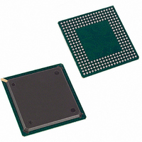
Manufacturer Part Number
DS21Q55
Description
IC TXRX QUAD T1/E1/J1 SCT 256BGA
Manufacturer
Maxim Integrated Products
Datasheet
1.DS21Q55.pdf
(237 pages)
Specifications of DS21Q55
Function
Transceiver
Interface
E1, J1, T1
Number Of Circuits
4
Voltage - Supply
3.14 V ~ 3.47 V
Current - Supply
75mA
Operating Temperature
0°C ~ 70°C
Mounting Type
Surface Mount
Package / Case
256-BGA
Includes
BERT Generator and Detector, Dual HDLC Controllers
Lead Free Status / RoHS Status
Contains lead / RoHS non-compliant
Power (watts)
-
Available stocks
Company
Part Number
Manufacturer
Quantity
Price

Company:
Part Number:
DS21Q552
Manufacturer:
DALLAS
Quantity:
319
Company:
Part Number:
DS21Q552BN+
Manufacturer:
Maxim Integrated
Quantity:
10 000
Part Number:
DS21Q554
Manufacturer:
DALLAS
Quantity:
20 000
Part Number:
DS21Q554B+
Manufacturer:
MAXIM/美信
Quantity:
20 000


Register Name:
Register Description:
Register Address:
Bit #
Name
Default
Bit 0/Transmit Alternate Ones and Zeros (TAOZ). Transmit a …101010… pattern (customer disconnect
indication signal) at TTIP and TRING. The transmission of this data pattern is always timed off of TCLK.
Bit 1/Transmit Synchronization G.703 Clock Enable (TSCLKE)
Bit 2/Receive Synchronization G.703 Clock Enable (RSCLKE)
Bits 3 to 4/Monitor Mode (MM0 to MM1)
Bit 5/Receive-Clock Edge Select (RCES). Selects which RCLKO edge to update RPOSO and RNEGO.
Bit 6/Transmit-Clock Edge Select (TCES). Selects which TCLKI edge to sample TPOSI and TNEGI.
Bit 7/Unused, must be set to 0 for proper operation
MM1
0
0
1
1
0 = disabled
1 = enabled
0 = disable 1.544MHz (T1)/2.048MHz (E1) transmit synchronization clock
1 = enable 1.544MHz (T1)/2.048MHz (E1) transmit synchronization clock
0 = disable 1.544MHz (T1)/2.048MHz (E1) synchronization receive mode
1 = enable 1.544MHz (T1)/2.048MHz (E1) synchronization receive mode
0 = update RPOSO and RNEGO on rising edge of RCLKO
1 = update RPOSO and RNEGO on falling edge of RCLKO
0 = sample TPOSI and TNEGI on falling edge of TCLKI
1 = sample TPOSI and TNEGI on rising edge of TCLKI
MM0
—
0
1
0
1
7
0
Normal operation (no boost)
20
26
32
Internal Linear Gain Boost
TCES
LIC3
Line Interface Control 3
7Ah
6
0
RCES
(dB)
5
0
MM1
4
0
155 of 237
MM0
3
0
RSCLKE TSCLKE
2
0
1
0
TAOZ
0
0
Related parts for DS21Q55
Image
Part Number
Description
Manufacturer
Datasheet
Request
R

Part Number:
Description:
MAX7528KCWPMaxim Integrated Products [CMOS Dual 8-Bit Buffered Multiplying DACs]
Manufacturer:
Maxim Integrated Products
Datasheet:
Part Number:
Description:
Single +5V, fully integrated, 1.25Gbps laser diode driver.
Manufacturer:
Maxim Integrated Products
Datasheet:
Part Number:
Description:
Single +5V, fully integrated, 155Mbps laser diode driver.
Manufacturer:
Maxim Integrated Products
Datasheet:
Part Number:
Description:
VRD11/VRD10, K8 Rev F 2/3/4-Phase PWM Controllers with Integrated Dual MOSFET Drivers
Manufacturer:
Maxim Integrated Products
Datasheet:
Part Number:
Description:
Highly Integrated Level 2 SMBus Battery Chargers
Manufacturer:
Maxim Integrated Products
Datasheet:
Part Number:
Description:
Current Monitor and Accumulator with Integrated Sense Resistor; ; Temperature Range: -40°C to +85°C
Manufacturer:
Maxim Integrated Products
Part Number:
Description:
TSSOP 14/A�/RS-485 Transceivers with Integrated 100O/120O Termination Resis
Manufacturer:
Maxim Integrated Products
Part Number:
Description:
TSSOP 14/A�/RS-485 Transceivers with Integrated 100O/120O Termination Resis
Manufacturer:
Maxim Integrated Products
Part Number:
Description:
QFN 16/A�/AC-DC and DC-DC Peak-Current-Mode Converters with Integrated Step
Manufacturer:
Maxim Integrated Products
Part Number:
Description:
TDFN/A/65V, 1A, 600KHZ, SYNCHRONOUS STEP-DOWN REGULATOR WITH INTEGRATED SWI
Manufacturer:
Maxim Integrated Products
Part Number:
Description:
Integrated Temperature Controller f
Manufacturer:
Maxim Integrated Products
Part Number:
Description:
SOT23-6/I�/45MHz to 650MHz, Integrated IF VCOs with Differential Output
Manufacturer:
Maxim Integrated Products
Part Number:
Description:
SOT23-6/I�/45MHz to 650MHz, Integrated IF VCOs with Differential Output
Manufacturer:
Maxim Integrated Products
Part Number:
Description:
EVALUATION KIT/2.4GHZ TO 2.5GHZ 802.11G/B RF TRANSCEIVER WITH INTEGRATED PA
Manufacturer:
Maxim Integrated Products
Part Number:
Description:
QFN/E/DUAL PCIE/SATA HIGH SPEED SWITCH WITH INTEGRATED BIAS RESISTOR
Manufacturer:
Maxim Integrated Products
Datasheet: