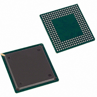
DS21Q55 Maxim Integrated Products, DS21Q55 Datasheet - Page 66

DS21Q55
Manufacturer Part Number
DS21Q55
Description
IC TXRX QUAD T1/E1/J1 SCT 256BGA
Manufacturer
Maxim Integrated Products
Datasheet
1.DS21Q55.pdf
(237 pages)
Specifications of DS21Q55
Function
Transceiver
Interface
E1, J1, T1
Number Of Circuits
4
Voltage - Supply
3.14 V ~ 3.47 V
Current - Supply
75mA
Operating Temperature
0°C ~ 70°C
Mounting Type
Surface Mount
Package / Case
256-BGA
Includes
BERT Generator and Detector, Dual HDLC Controllers
Lead Free Status / RoHS Status
Contains lead / RoHS non-compliant
Power (watts)
-
Available stocks
Company
Part Number
Manufacturer
Quantity
Price
Company:
Part Number:
DS21Q552
Manufacturer:
DALLAS
Quantity:
319
Company:
Part Number:
DS21Q552BN+
Manufacturer:
Maxim Integrated
Quantity:
10 000
Part Number:
DS21Q554
Manufacturer:
DALLAS
Quantity:
20 000
Part Number:
DS21Q554B+
Manufacturer:
MAXIM/美信
Quantity:
20 000
9. COMMON CONTROL AND STATUS REGISTERS
Register Name:
Register Description:
Register Address:
Bit #
Name
Default
Bit 0/Function of the RLOS/LOTC Output (RLOSF)
Bit 1/Transmit Clock Source Select Bit 0 (TCSS0)
Bit 2/Transmit Clock Source Select Bit 0 (TCSS1)
Bit 3/Disable Idle Code Auto Increment (DICAI). Selects/deselects the auto-increment feature for the transmit
and receive idle code array address register. See Section 15.
Bit 4/Output Data Mode (ODM)
Bit 5/Signaling Integration Enable (SIE)
Bit 6/CRC-4 Recalculate (CRC4R)
Bit 7/MCLK Source (MCLKS). Selects the source of MCLK
TCSS1
0
0
1
1
0 = receive loss of sync (RLOS)
1 = loss-of-transmit clock (LOTC)
0 = addresses in IAAR register automatically increment on every read/write operation to the PCICR
register
1 = addresses in IAAR register do not automatically increment
0 = pulses at TPOSO and TNEGO are one full TCLKO period wide
1 = pulses at TPOSO and TNEGO are one-half TCLKO period wide
0 = signaling changes of state reported on any change in selected channels
1 = signaling must be stable for three multiframes in order for a change of state to be reported
0 = transmit CRC-4 generation and insertion operates in normal mode
1 = transmit CRC-4 generation operates according to G.706 intermediate path recalculation method
0 = MCLK is source from the MCLK pin
1 = MCLK is source from the TSYSCLK pin
MCLKS
TCSS0
7
0
0
1
0
1
CRC4R
CCR1
Common Control Register 1
70h
The TCLK pin is always the source of transmit clock.
Switch to the clock present at RCLK when the signal at the TCLK pin
fails to transition after 1 channel time.
Use the scaled signal present at MCLK as the transmit clock. The
TCLK pin is ignored.
Use the signal present at RCLK as the transmit clock. The TCLK pin is
ignored.
6
0
SIE
5
0
ODM
4
0
Transmit Clock Source
66 of 237
DICAI
3
0
TCSS1
2
0
TCSS0
1
0
RLOSF
0
0


