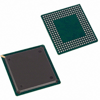
DS21Q55 Maxim Integrated Products, DS21Q55 Datasheet - Page 223

DS21Q55
Manufacturer Part Number
DS21Q55
Description
IC TXRX QUAD T1/E1/J1 SCT 256BGA
Manufacturer
Maxim Integrated Products
Datasheet
1.DS21Q55.pdf
(237 pages)
Specifications of DS21Q55
Function
Transceiver
Interface
E1, J1, T1
Number Of Circuits
4
Voltage - Supply
3.14 V ~ 3.47 V
Current - Supply
75mA
Operating Temperature
0°C ~ 70°C
Mounting Type
Surface Mount
Package / Case
256-BGA
Includes
BERT Generator and Detector, Dual HDLC Controllers
Lead Free Status / RoHS Status
Contains lead / RoHS non-compliant
Power (watts)
-
Available stocks
Company
Part Number
Manufacturer
Quantity
Price
Company:
Part Number:
DS21Q552
Manufacturer:
DALLAS
Quantity:
319
Company:
Part Number:
DS21Q552BN+
Manufacturer:
Maxim Integrated
Quantity:
10 000
Part Number:
DS21Q554
Manufacturer:
DALLAS
Quantity:
20 000
Part Number:
DS21Q554B+
Manufacturer:
MAXIM/美信
Quantity:
20 000
33.
Capacitive test loads are 30pF for bus signals, 20pF for all others.
33.1 Multiplexed Bus AC Characteristics
AC CHARACTERISTICS: MULTIPLEXED PARALLEL PORT (MUX = 1)
(Figure
(V
Cycle Time
Pulse Width, DS Low or RD High
Pulse Width, DS High or RD Low
Input Rise/Fall Times
R/W Hold Time
R/W Setup Time Before DS High
CS Setup Time Before DS, WR, or RD
Active
CS Hold Time
Read Data-Hold Time
Write Data-Hold Time
Muxed Address Valid to AS or ALE Fall
Muxed Address Hold Time
Delay Time DS, WR, or RD to AS or ALE
Rise
Pulse Width AS or ALE High
Delay Time, AS or ALE to DS, WR, or RD
Output Data Delay Time from DS or RD
Data Setup Time
DD
= 3.3V ±5%, T
AC TIMING PARAMETERS AND DIAGRAMS
33-1,
PARAMETER
Figure
A
= 0°C to +70°C for DS21Q55; V
33-2, and
Figure
33-3)
SYMBOL
PW
PW
PW
t
t
t
t
t
t
t
t
t
t
t
t
ASED
R
RWH
DHW
RWS
t
t
DDR
DSW
CYC
DHR
AHL
ASD
ASL
CH
CS
, t
ASH
223 of 237
EH
EL
DD
F
= 3.3V ±5%, T
CONDITIONS
A
= -40°C to +85°C for DS21Q55N.)
MIN
200
100
100
10
50
20
10
15
10
20
30
10
20
50
0
0
TYP
MAX
20
50
80
UNITS
ns
ns
ns
ns
ns
ns
ns
ns
ns
ns
ns
ns
ns
ns
ns
ns
ns


