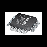
LPC11U13FBD48 NXP Semiconductors, LPC11U13FBD48 Datasheet - Page 9

LPC11U13FBD48
Manufacturer Part Number
LPC11U13FBD48
Description
The LPC11U13FBD48 is a ARM Cortex-M0 based, low-cost 32-bit MCU, designed for 8/16-bit microcontroller applications, offering performance, low power, simple instruction set and memory addressing together with reduced code size compared to existing 8/
Manufacturer
NXP Semiconductors
Datasheet
1.LPC11U12FBD48.pdf
(69 pages)
Available stocks
Company
Part Number
Manufacturer
Quantity
Price
Company:
Part Number:
LPC11U13FBD48/201
Manufacturer:
NXP
Quantity:
1 000
Company:
Part Number:
LPC11U13FBD48/201,
Manufacturer:
NXP Semiconductors
Quantity:
10 000
NXP Semiconductors
Table 3.
LPC11U1X
Product data sheet
Symbol
PIO0_5/SDA
PIO0_6/USB_CONNECT/
SCK0
PIO0_7/CTS
PIO0_8/MISO0/
CT16B0_MAT0
PIO0_9/MOSI0/
CT16B0_MAT1
SWCLK/PIO0_10/SCK0/
CT16B0_MAT2
TDI/PIO0_11/AD0/
CT32B0_MAT3
Pin description
11
15
16
17
18
19
21
16
22
23
27
28
29
32
All information provided in this document is subject to legal disclaimers.
H3
H6
G7
F8
F7
E7
D8
Rev. 2 — 11 January 2012
[4]
[3]
[5]
[3]
[3]
[3]
[6]
Reset
state
[1]
I; IA
-
I; PU
-
-
I; PU
-
I; PU
-
-
I; PU
-
-
I; PU
-
-
-
I; PU
-
-
-
Type
I/O
I/O
I/O
O
I/O
I/O
I
I/O
I/O
O
I/O
I/O
O
I
I/O
O
O
I
I/O
I
O
Description
PIO0_5 — General purpose digital input/output
pin (open-drain).
SDA — I
High-current sink only if I
selected in the I/O configuration register.
PIO0_6 — General purpose digital input/output
pin.
USB_CONNECT — Signal used to switch an
external 1.5 k resistor under software control.
Used with the SoftConnect USB feature.
SCK0 — Serial clock for SSP0.
PIO0_7 — General purpose digital input/output
pin (high-current output driver).
CTS — Clear To Send input for USART.
PIO0_8 — General purpose digital input/output
pin.
MISO0 — Master In Slave Out for SSP0.
CT16B0_MAT0 — Match output 0 for 16-bit
timer 0.
PIO0_9 — General purpose digital input/output
pin.
MOSI0 — Master Out Slave In for SSP0.
CT16B0_MAT1 — Match output 1 for 16-bit
timer 0.
SWCLK — Serial wire clock and test clock TCK
for JTAG interface.
PIO0_10 — General purpose digital
input/output pin.
SCK0 — Serial clock for SSP0.
CT16B0_MAT2 — Match output 2 for 16-bit
timer 0.
TDI — Test Data In for JTAG interface.
PIO0_11 — General purpose digital input/output
pin.
AD0 — A/D converter, input 0.
CT32B0_MAT3 — Match output 3 for 32-bit
timer 0.
32-bit ARM Cortex-M0 microcontroller
2
C-bus data input/output (open-drain).
LPC11U1x
2
C Fast-mode Plus is
© NXP B.V. 2012. All rights reserved.
9 of 69


