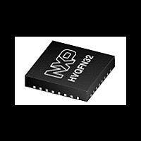
LPC11U14FHI33 NXP Semiconductors, LPC11U14FHI33 Datasheet - Page 14

LPC11U14FHI33
Manufacturer Part Number
LPC11U14FHI33
Description
The LPC11U14FHI33 is a ARM Cortex-M0 based, low-cost 32-bit MCU, designed for 8/16-bit microcontroller applications, offering performance, low power, simple instruction set and memory addressing together with reduced code size compared to existing 8/
Manufacturer
NXP Semiconductors
Datasheet
1.LPC11U12FBD48.pdf
(69 pages)
NXP Semiconductors
[1]
[3]
[4]
[5]
[6]
[7]
[8]
Table 4.
LPC11U1X
Product data sheet
[2]
Peripheral
USART
SSP0
SSP1
CT16B0
Pin state at reset for default function: I = Input; O = Output; PU = internal pull-up enabled; IA = inactive, no pull-up/down enabled;
F = floating; floating pins, if not used, should be tied to ground or power to minimize power consumption.
See
reset the chip and wake up from Deep power-down mode. An external pull-up resistor is required on this pin for the Deep power-down
mode.
5 V tolerant pad providing digital I/O functions with configurable pull-up/pull-down resistors and configurable hysteresis (see
I
5 V tolerant pad providing digital I/O functions with configurable pull-up/pull-down resistors and configurable hysteresis (see
includes high-current output driver.
5 V tolerant pad providing digital I/O functions with configurable pull-up/pull-down resistors, configurable hysteresis, and analog input.
When configured as a ADC input, digital section of the pad is disabled and the pin is not 5 V tolerant (see
input glitch filter.
Pad provides USB functions. It is designed in accordance with the USB specification, revision 2.0 (Full-speed and Low-speed mode
only). This pad is not 5 V tolerant.
When the system oscillator is not used, connect XTALIN and XTALOUT as follows: XTALIN can be left floating or can be grounded
(grounding is preferred to reduce susceptibility to noise). XTALOUT should be left floating.
2
C-bus pins compliant with the I
Figure 30
Multiplexing of peripheral functions
Function
TXD
CTS
RTS
DTR
DSR
DCD
RI
SCLK
SCK0
SSEL0
MISO0
MOSI0
SCK1
SSEL1
MISO1
MOSI1
CT16B0_CAP0
CT16B0_MAT0
CT16B0_MAT1
CT16B0_MAT2
RXD
for the reset pad configuration. RESET functionality is not available in Deep power-down mode. Use the WAKEUP pin to
To assign a peripheral function to a port, program the FUNC bits in the port pin’s IOCON
register with this function. The user must ensure that the assignment of a function to a port
pin is unambiguous. Only the debug functions for JTAG and SWD are selected by default
in their corresponding IOCON registers. All other functions must be programmed in the
IOCON block before they can be used. For details see the LPC11Uxx user manual.
2
Type Default Available on ports
I
O
I
O
O
I
I
I
I/O
I/O
I/O
I/O
I/O
I/O
I/O
I/O
I/O
I
O
O
O
C-bus specification for I
no
no
no
no
no
no
no
no
no
no
no
no
no
no
no
no
no
no
no
no
no
All information provided in this document is subject to legal disclaimers.
Rev. 2 — 11 January 2012
HVQFN33/LQFP48/TFBGA48 LQFP48/TFBGA48
PIO0_18
PIO0_19
PIO0_7
PIO0_17
PIO1_13
-
PIO1_15
-
PIO0_17
PIO0_6
PIO0_2
PIO0_8
PIO0_9
PIO1_15
PIO1_19
PIO0_22
PIO0_21
PIO0_2
PIO0_8
PIO0_9
PIO0_10
2
C standard mode, I
-
-
-
-
PIO1_19
-
PIO0_10
-
-
-
-
-
-
-
-
-
-
PIO1_15
2
C Fast-mode, and I
32-bit ARM Cortex-M0 microcontroller
PIO1_14
PIO1_13
-
-
-
PIO1_14
PIO1_21
PIO1_16
PIO1_28
PIO1_29
-
-
-
PIO1_20
PIO1_23
PIO1_21
PIO1_22
PIO1_16
PIO1_13
PIO1_14
-
2
C Fast-mode Plus.
PIO1_26
PIO1_27
-
-
-
PIO1_20
-
PIO1_22
-
-
-
-
-
-
-
-
-
-
-
-
Figure
LPC11U1x
© NXP B.V. 2012. All rights reserved.
29); includes digital
TFBGA48
-
-
-
-
-
-
-
-
-
-
-
-
-
-
-
-
-
-
-
-
-
Figure
Figure
14 of 69
29);
29).


