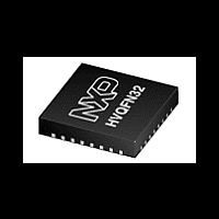
LPC11U14FHI33 NXP Semiconductors, LPC11U14FHI33 Datasheet - Page 29

LPC11U14FHI33
Manufacturer Part Number
LPC11U14FHI33
Description
The LPC11U14FHI33 is a ARM Cortex-M0 based, low-cost 32-bit MCU, designed for 8/16-bit microcontroller applications, offering performance, low power, simple instruction set and memory addressing together with reduced code size compared to existing 8/
Manufacturer
NXP Semiconductors
Datasheet
1.LPC11U12FBD48.pdf
(69 pages)
- Current page: 29 of 69
- Download datasheet (2Mb)
NXP Semiconductors
LPC11U1X
Product data sheet
7.17 Emulation and debugging
Debug functions are integrated into the ARM Cortex-M0. Serial wire debug functions are
supported in addition to a standard JTAG boundary scan. The ARM Cortex-M0 is
configured to support up to four breakpoints and two watch points.
The RESET pin selects between the JTAG boundary scan (RESET = LOW) and the ARM
SWD debug (RESET = HIGH). The ARM SWD debug port is disabled while the
LPC11U1x is in reset.
To perform boundary scan testing, follow these steps:
Remark: The JTAG interface cannot be used for debug purposes.
1. Erase any user code residing in flash.
2. Power up the part with the RESET pin pulled HIGH externally.
3. Wait for at least 250 s.
4. Pull the RESET pin LOW externally.
5. Perform boundary scan operations.
6. Once the boundary scan operations are completed, assert the TRST pin to enable the
SWD debug mode and release the RESET pin (pull HIGH).
All information provided in this document is subject to legal disclaimers.
Rev. 2 — 11 January 2012
32-bit ARM Cortex-M0 microcontroller
LPC11U1x
© NXP B.V. 2012. All rights reserved.
29 of 69
Related parts for LPC11U14FHI33
Image
Part Number
Description
Manufacturer
Datasheet
Request
R
Part Number:
Description:
LPC11U14 XPRESSO BOARD
Manufacturer:
NXP Semiconductors
Datasheet:
Part Number:
Description:
Development Boards & Kits - ARM NGX LPC11U1x Eval Board
Manufacturer:
NXP Semiconductors
Part Number:
Description:
LPC1114FBD48/LQFP48/REEL13//30
Manufacturer:
NXP Semiconductors
Datasheet:
Part Number:
Description:
NXP Semiconductors designed the LPC2420/2460 microcontroller around a 16-bit/32-bitARM7TDMI-S CPU core with real-time debug interfaces that include both JTAG andembedded trace
Manufacturer:
NXP Semiconductors
Datasheet:

Part Number:
Description:
NXP Semiconductors designed the LPC2458 microcontroller around a 16-bit/32-bitARM7TDMI-S CPU core with real-time debug interfaces that include both JTAG andembedded trace
Manufacturer:
NXP Semiconductors
Datasheet:
Part Number:
Description:
NXP Semiconductors designed the LPC2468 microcontroller around a 16-bit/32-bitARM7TDMI-S CPU core with real-time debug interfaces that include both JTAG andembedded trace
Manufacturer:
NXP Semiconductors
Datasheet:
Part Number:
Description:
NXP Semiconductors designed the LPC2470 microcontroller, powered by theARM7TDMI-S core, to be a highly integrated microcontroller for a wide range ofapplications that require advanced communications and high quality graphic displays
Manufacturer:
NXP Semiconductors
Datasheet:
Part Number:
Description:
NXP Semiconductors designed the LPC2478 microcontroller, powered by theARM7TDMI-S core, to be a highly integrated microcontroller for a wide range ofapplications that require advanced communications and high quality graphic displays
Manufacturer:
NXP Semiconductors
Datasheet:
Part Number:
Description:
The Philips Semiconductors XA (eXtended Architecture) family of 16-bit single-chip microcontrollers is powerful enough to easily handle the requirements of high performance embedded applications, yet inexpensive enough to compete in the market for hi
Manufacturer:
NXP Semiconductors
Datasheet:
Part Number:
Description:
The XA-S3 device is a member of Philips Semiconductors? XA(eXtended Architecture) family of high performance 16-bitsingle-chip microcontrollers
Manufacturer:
NXP Semiconductors
Datasheet:

Part Number:
Description:
The NXP BlueStreak LH75401/LH75411 family consists of two low-cost 16/32-bit System-on-Chip (SoC) devices
Manufacturer:
NXP Semiconductors
Datasheet:

Part Number:
Description:
The NXP LPC3130/3131 combine an 180 MHz ARM926EJ-S CPU core, high-speed USB2
Manufacturer:
NXP Semiconductors
Datasheet:

Part Number:
Description:
The NXP LPC3141 combine a 270 MHz ARM926EJ-S CPU core, High-speed USB 2
Manufacturer:
NXP Semiconductors

Part Number:
Description:
The NXP LPC3143 combine a 270 MHz ARM926EJ-S CPU core, High-speed USB 2
Manufacturer:
NXP Semiconductors


