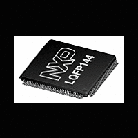
LPC2926_27_29 NXP Semiconductors, LPC2926_27_29 Datasheet - Page 12

LPC2926_27_29
Manufacturer Part Number
LPC2926_27_29
Description
The LPC2926/2927/2929 combine an ARM968E-S CPU core with two integrated TCMblocks operating at frequencies of up to 125 MHz, Full-speed USB 2
Manufacturer
NXP Semiconductors
Datasheet
1.LPC2926_27_29.pdf
(95 pages)
NXP Semiconductors
LPC2926_27_29
Product data sheet
6.2 ARM968E-S processor
The LPC2926/2927/2929 configures the ARM968E-S processor in little-endian byte order.
All peripherals run at their own clock frequency to optimize the total system power
consumption. The AHB-to-APB bridge used in the subsystems contains a write-ahead
buffer one transaction deep. This implies that when the ARM968E-S issues a buffered
write action to a register located on the APB side of the bridge, it continues even though
the actual write may not yet have taken place. Completion of a second write to the same
subsystem will not be executed until the first write is finished.
The ARM968E-S is a general purpose 32-bit RISC processor, which offers high
performance and very low power consumption. The ARM architecture is based on
Reduced Instruction Set Computer (RISC) principles, and the instruction set and related
decode mechanism are much simpler than those of microprogrammed Complex
Instruction Set Computers (CISC). This simplicity results in a high instruction throughput
and impressive real-time interrupt response from a small and cost-effective controller
core.
Amongst the most compelling features of the ARM968E-S are:
Pipeline techniques are employed so that all parts of the processing and memory systems
can operate continuously. The ARM968E-S is based on the ARMv5TE five-stage pipeline
architecture. Typically, in a three-stage pipeline architecture, while one instruction is being
executed its successor is being decoded and a third instruction is being fetched from
memory. In the five-stage pipeline additional stages are added for memory access and
write-back cycles.
The ARM968E-S processor also employs a unique architectural strategy known as
THUMB, which makes it ideally suited to high-volume applications with memory
restrictions or to applications where code density is an issue.
The key idea behind THUMB is that of a super-reduced instruction set. Essentially, the
ARM968E-S processor has two instruction sets:
The THUMB set's 16-bit instruction length allows it to approach twice the density of
standard ARM code while retaining most of the ARM's performance advantage over a
traditional 16-bit controller using 16-bit registers. This is possible because THUMB code
operates on the same 32-bit register set as ARM code.
THUMB code can provide up to 65 % of the code size of ARM, and 160 % of the
performance of an equivalent ARM controller connected to a 16-bit memory system.
The ARM968E-S processor is described in detail in the ARM968E-S data sheet
•
•
•
•
•
Separate directly connected instruction and data Tightly Coupled Memory (TCM)
interfaces
Write buffers for the AHB and TCM buses
Enhanced 16 × 32 multiplier capable of single-cycle MAC operations and 16-bit fixed-
point DSP instructions to accelerate signal-processing algorithms and applications.
Standard 32-bit ARMv5TE set
16-bit THUMB set
All information provided in this document is subject to legal disclaimers.
Rev. 5 — 28 September 2010
ARM9 microcontroller with CAN, LIN, and USB
LPC2926/2927/2929
© NXP B.V. 2010. All rights reserved.
Ref.
12 of 95
2.


