LPC2926_27_29 NXP Semiconductors, LPC2926_27_29 Datasheet - Page 30

LPC2926_27_29
Manufacturer Part Number
LPC2926_27_29
Description
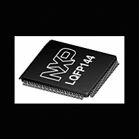
The LPC2926/2927/2929 combine an ARM968E-S CPU core with two integrated TCMblocks operating at frequencies of up to 125 MHz, Full-speed USB 2
Manufacturer
NXP Semiconductors
Datasheet
1.LPC2926_27_29.pdf
(95 pages)
- Current page: 30 of 95
- Download datasheet (2Mb)
NXP Semiconductors
LPC2926_27_29
Product data sheet
6.12.4.1 Pin description
6.13.1 Peripheral subsystem clock description
6.13.2 Watchdog timer
6.13 Peripheral subsystem
The event router module in the LPC2926/2927/2929 is connected to the pins listed below.
The pins are combined with other functions on the port pins of the LPC2926/2927/2929.
Table 15
Table 15.
The peripheral subsystem is clocked by a number of different clocks:
The purpose of the watchdog timer is to reset the ARM9 processor within a reasonable
amount of time if the processor enters an error state. The watchdog generates a system
reset if the user program fails to trigger it correctly within a predetermined amount of time.
Key features:
Symbol
EXTINT[0:7]
CAN0 RXD
CAN1 RXD
I2C0_SCL
I2C1_SCL
LIN0 RXD
LIN1 RXD
SPI0 SDI
SPI1 SDI
SPI2 SDI
UART0 RXD
UART1 RXD
USB_SCL
-
-
-
•
•
•
•
•
•
•
•
CLK_SYS_PESS
CLK_UART0/1
CLK_SPI0/1/2
CLK_TMR0/1/2/3
CLK_SAFE see
Internal chip reset if not periodically triggered
Timer counter register runs on always-on safe clock
Optional interrupt generation on watchdog time-out
shows the pins connected to the event router.
Event-router pin connections
All information provided in this document is subject to legal disclaimers.
Direction
I
I
I
I
I
I
I
I
I
I
I
I
I
n/a
n/a
n/a
Section 6.7.2
Rev. 5 — 28 September 2010
Description
external interrupt input 0 to 7
CAN0 receive data input wake-up
CAN1 receive data input wake-up
I2C0 SCL clock input
I2C1 SCL clock input
LIN0 receive data input wake-up
LIN1 receive data input wake-up
SPI0 receive data input
SPI1 receive data input
SPI2 receive data input
UART0 receive data input
UART1 receive data input
USB I
CAN interrupt (internal)
VIC FIQ (internal)
VIC IRQ (internal)
2
ARM9 microcontroller with CAN, LIN, and USB
C-bus serial clock
LPC2926/2927/2929
© NXP B.V. 2010. All rights reserved.
Default polarity
1
0
0
0
0
0
0
0
0
0
0
0
0
1
1
1
30 of 95
Related parts for LPC2926_27_29
Image
Part Number
Description
Manufacturer
Datasheet
Request
R
Part Number:
Description:
Lpc2926/2927/2929 Arm9 Microcontroller With Can, Lin, And Usb
Manufacturer:
NXP Semiconductors
Datasheet:
Part Number:
Description:
NXP Semiconductors designed the LPC2420/2460 microcontroller around a 16-bit/32-bitARM7TDMI-S CPU core with real-time debug interfaces that include both JTAG andembedded trace
Manufacturer:
NXP Semiconductors
Datasheet:

Part Number:
Description:
NXP Semiconductors designed the LPC2458 microcontroller around a 16-bit/32-bitARM7TDMI-S CPU core with real-time debug interfaces that include both JTAG andembedded trace
Manufacturer:
NXP Semiconductors
Datasheet:
Part Number:
Description:
NXP Semiconductors designed the LPC2468 microcontroller around a 16-bit/32-bitARM7TDMI-S CPU core with real-time debug interfaces that include both JTAG andembedded trace
Manufacturer:
NXP Semiconductors
Datasheet:
Part Number:
Description:
NXP Semiconductors designed the LPC2470 microcontroller, powered by theARM7TDMI-S core, to be a highly integrated microcontroller for a wide range ofapplications that require advanced communications and high quality graphic displays
Manufacturer:
NXP Semiconductors
Datasheet:
Part Number:
Description:
NXP Semiconductors designed the LPC2478 microcontroller, powered by theARM7TDMI-S core, to be a highly integrated microcontroller for a wide range ofapplications that require advanced communications and high quality graphic displays
Manufacturer:
NXP Semiconductors
Datasheet:
Part Number:
Description:
The Philips Semiconductors XA (eXtended Architecture) family of 16-bit single-chip microcontrollers is powerful enough to easily handle the requirements of high performance embedded applications, yet inexpensive enough to compete in the market for hi
Manufacturer:
NXP Semiconductors
Datasheet:
Part Number:
Description:
The XA-S3 device is a member of Philips Semiconductors? XA(eXtended Architecture) family of high performance 16-bitsingle-chip microcontrollers
Manufacturer:
NXP Semiconductors
Datasheet:

Part Number:
Description:
The NXP BlueStreak LH75401/LH75411 family consists of two low-cost 16/32-bit System-on-Chip (SoC) devices
Manufacturer:
NXP Semiconductors
Datasheet:

Part Number:
Description:
The NXP LPC3130/3131 combine an 180 MHz ARM926EJ-S CPU core, high-speed USB2
Manufacturer:
NXP Semiconductors
Datasheet:

Part Number:
Description:
The NXP LPC3141 combine a 270 MHz ARM926EJ-S CPU core, High-speed USB 2
Manufacturer:
NXP Semiconductors

Part Number:
Description:
The NXP LPC3143 combine a 270 MHz ARM926EJ-S CPU core, High-speed USB 2
Manufacturer:
NXP Semiconductors

Part Number:
Description:
The NXP LPC3152 combines an 180 MHz ARM926EJ-S CPU core, High-speed USB 2
Manufacturer:
NXP Semiconductors

Part Number:
Description:
The NXP LPC3154 combines an 180 MHz ARM926EJ-S CPU core, High-speed USB 2
Manufacturer:
NXP Semiconductors


