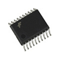
FMS6407MTC20 Fairchild Semiconductor, FMS6407MTC20 Datasheet - Page 12

FMS6407MTC20
Manufacturer Part Number
FMS6407MTC20
Description
IC DRVR VID TRPL W/FLTRS 20TSSOP
Manufacturer
Fairchild Semiconductor
Type
Driverr
Datasheet
1.FMS6407MTC20X.pdf
(17 pages)
Specifications of FMS6407MTC20
Applications
Recorders, Set-Top Boxes
Mounting Type
Surface Mount
Package / Case
20-TSSOP
Lead Free Status / RoHS Status
Lead free / RoHS Compliant
Other names
FMS6407MTC20_NL
FMS6407MTC20_NL
FMS6407MTC20_NL
Available stocks
Company
Part Number
Manufacturer
Quantity
Price
Part Number:
FMS6407MTC20
Manufacturer:
FAIRCHILD/仙童
Quantity:
20 000
Company:
Part Number:
FMS6407MTC20X
Manufacturer:
FUJI
Quantity:
72
Part Number:
FMS6407MTC20X
Manufacturer:
FAIRCHILD/仙童
Quantity:
20 000
DATA SHEET
12
Note: Timing values are approximate for 30Hz/60Hz refresh rates.
Application Information
Input Circuitry
The DC restore circuit in the FMS6407 requires a source
impedance (R
for correct operation. Driving the FMS6407 with a high-
impedance source (e.g. a DAC loaded with 330Ω) will not
yield optimum results.
Output Drive
The FMS6407 is specified to operate with output currents
typically less than 60mA, more than sufficient for a dual
(75Ω) video load. Internal amplifiers are current limited to
approximately 100mA and should withstand brief duration
short circuit conditions, however this capability is not
guaranteed.
The maximum specified input voltage of 1.5V
tained for all inputs. When the input is clamped to 1.125V,
this does not result in a meaningful output signal. With a
gain of 6dB, the output should be 1.125V ±1.5V which is not
possible since the output cannot drive below ground. This
condition will not damage the part; however, the output will
be clipped. For signals which are clamped to 250mV, this
does not occur.
Signals that are at midscale during SYNC (Pb, Pr, C) must
be clamped to 1.125V and signals that are at their lowest
during SYNC (Y, CV, R, G, B) must be clamped to 250mV
Filter Settings
Table I
Format
1080i
480p
720p
480i
F
SEL1
, Pin 10
0
0
1
1
Refresh
source
30Hz
60Hz
60Hz
30Hz
= R
s
|| R
F
Sample Rate
T
SEL0
74.25MHz
74.25MHz
) of less than or equal to 150Ω
13.5MHz
27MHz
, Pin 9
0
1
0
1
Period (T)
13.4ns
13.4ns
Filter -3dB Freq
pp
74ns
37ns
Filter Bypass
can be sus-
8.2MHz
15MHz
32MHz
20T = 750ns
70T = 938ns
44T = 589ns
20T = 1.5µs
for proper operation. Clamping a CV signal to 1.125V will
result in clipping the top of the signal and clamping a Pr sig-
nal to 250mV will result in clipping the bottom of the signal.
The 220µF capacitor coupled with the 150Ω termination, as
shown in the Typical Application Circuit of Figure 5, forms a
high pass filter that blocks the DC while passing the video
frequencies and avoiding tilt. Any value lower than 220µF
will create problems, such as video tilt. Higher values, such
as 470µF - 1000µF are the most optimal output coupling
capacitor. By AC coupling, the average DC level is zero.
Thus, the output voltages of all channels will be centered
around zero.
Sync Recovery
The FMS6407 will typically recover bi-level sync with
amplitude greater than 100mV (33% compressed relative to
the nominal 300mV amplitude). The FMS6407 looks for the
lowest signal voltage and clamps this to approximately
250mV at the output.
Tri-level sync may not be compressed more than 5% (15mV)
for correct operation. Tri-level sync is located by finding the
edges of the tri-level pulse and running a timer to operate the
clamp during the back porch interval.
Since only the Y/G channel is processed for sync recovery, Y
and CV inputs must be synchronous.
A
HD, 1080i, 720p
Video Format
PS, 480p
SD, 480i
64T = 2.35µs
40T = 536ns
44T = 589ns
64T = 4.7µs
–
B
Bi-level, 2.35µs pulse width
Bi-level, 2.35µs pulse width
Tri-level, 589ns pulse width
Bi-level, 4.7µs pulse width
220T = 2.95µs
148T = 1.98µs
61T = 2.25µs
61T = 4.5µs
Sync Format
C
REV. 1I July 2005
15.75kHz
33.75kHz
31.5kHz
H-Rate
45kHz
FMS6407


