74LCXR162245MEA Fairchild Semiconductor, 74LCXR162245MEA Datasheet

IC TXRX BIDIR 16BIT LV 48SSOP

74LCXR162245MEA

Manufacturer Part Number
74LCXR162245MEA
Description
IC TXRX BIDIR 16BIT LV 48SSOP
Manufacturer
Fairchild Semiconductor
Series
74LCXr
Datasheet

Specifications of 74LCXR162245MEA

Logic Type
Transceiver, Non-Inverting
Number Of Elements
2
Number Of Bits Per Element
8
Current - Output High, Low
12mA, 12mA
Voltage - Supply
2 V ~ 3.6 V
Operating Temperature
-40°C ~ 85°C
Mounting Type
Surface Mount
Package / Case
48-SSOP
Lead Free Status / RoHS Status
Lead free / RoHS Compliant
© 2005 Fairchild Semiconductor Corporation
Print form created on June 10, 2005 12:56 pm
74LCXR162245MEA
74LCXR162245MEX
74LCXR162245MTD
74LCXR162245MTX
74LCXR162245
Low Voltage 16-Bit Bidirectional Transceiver
with 5V Tolerant Inputs/Outputs
and 26: Series Resistors in the Outputs
General Description
The LCXR162245 contains sixteen non-inverting bidirec-
tional buffers with 3-STATE outputs and is intended for bus
oriented applications. The device is designed for low volt-
age (2.5V or 3.3V) V
facing to a 5V signal environment. The device is byte
controlled. Each byte has separate control inputs which
could be shorted together for full 16-bit operation. The T/R
inputs determine the direction of data flow through the
device. The OE inputs disable both the A and B ports by
placing them in a high impedance state.
In addition, all A and B outputs include equivalent 26
(nominal) series resistors to reduce overshoot and under-
shoot and are designed to sink/source up to 12 mA at
V
The LCXR162245 is fabricated with an advanced CMOS
technology to achieve high speed operation while maintain-
ing CMOS low power dissipation.
Ordering Code:
Devices also available in Tape and Reel. Specify by appending the suffix letter “x” to the ordering code.
Logic Symbol
CC
Order Number
3.0V.
CC
Package Number
applications with capability of inter-
MS48A
MS48A
MTD48
MTD48
48-Lead Small Shrink Outline Package (SSOP), JEDEC MO-118, 0.300" Wide
[RAIL]
48-Lead Small Shrink Outline Package (SSOP), JEDEC MO-118, 0.300" Wide
[TAPE and REEL]
48-Lead Thin Shrink Small Outline Package (TSSOP), JEDEC MO-153, 6.1mm Wide
[RAIL]
48-Lead Thin Shrink Small Outline Package (TSSOP), JEDEC MO-153, 6.1mm Wide
[TAPE and REEL]
DS500052
:
Features
Note 1: To ensure the high-impedance state during power up or down OE
should be tied to V
resistor is determined by the current-sourcing capability of the driver.
Pin Descriptions
OE
T/R
A
B
Pin Names
0
0
5V tolerant inputs and outputs
2.3V–3.6V V
A and B side outputs have equivalent 26
resistors
5.3 ns t
Power down high impedance inputs and outputs
Supports live insertion/withdrawal (Note 1)
Flow through pinout
Implements patented noise/EMI reduction circuitry
Latch-up performance exceeds 500 mA
ESD performance:
–A
–B
n
n
Human body model
Machine model
15
15
Package Description
PD
max (V
CC
CC
Output Enable Input
Transmit/Receive Input
Side A Inputs or 3-STATE Outputs
Side B Inputs or 3-STATE Outputs
through a pull-up resistor: the minimum value or the
specifications provided
CC
!
200V
!
3.3V), 20
2000V
August 1998
Revised June 2005
Description
P
A I
CC
www.fairchildsemi.com
max
:
series

Related parts for 74LCXR162245MEA

74LCXR162245MEA Summary of contents

Page 1

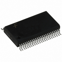
... The LCXR162245 is fabricated with an advanced CMOS technology to achieve high speed operation while maintain- ing CMOS low power dissipation. Ordering Code: Order Number Package Number 74LCXR162245MEA MS48A 48-Lead Small Shrink Outline Package (SSOP), JEDEC MO-118, 0.300" Wide [RAIL] 74LCXR162245MEX MS48A 48-Lead Small Shrink Outline Package (SSOP), JEDEC MO-118, 0.300" Wide ...

Page 2

Connection Diagram Logic Diagram www.fairchildsemi.com Truth Tables Inputs Outputs OE T Bus B –B Data to Bus Bus A –A Data to Bus HIGH Z State ...

Page 3

Absolute Maximum Ratings Symbol Parameter V Supply Voltage Input Voltage Output Voltage Input Diode Current Output Diode Current Output Source/Sink Current Supply ...

Page 4

DC Electrical Characteristics Symbol Parameter I Power-Off Leakage Current OFF I Quiescent Supply Current Increase in I per Input CC CC Note 6: Outputs disabled or 3-STATE only. AC Electrical Characteristics Symbol Parameter t Propagation Delay PHL ...

Page 5

AC LOADING and WAVEFORMS FIGURE 1. AC Test Circuit (C Test t PLH t PZL t PZH Waveform for Inverting and Non-Inverting Functions Propagation Delay. Pulse Width and t rec 3-STATE Output Low Enable and Disable Times for Logic (Input ...

Page 6

Schematic Diagram Generic for LCX Family www.fairchildsemi.com 6 ...

Page 7

Physical Dimensions inches (millimeters) unless otherwise noted 48-Lead Small Shrink Outline Package (SSOP), JEDEC MO-118, 0.300" Wide Package Number MS48A 7 www.fairchildsemi.com ...

Page 8

Physical Dimensions inches (millimeters) unless otherwise noted (Continued) 48-Lead Thin Shrink Small Outline Package (TSSOP), JEDEC MO-153, 6.1mm Wide Fairchild does not assume any responsibility for use of any circuitry described, no circuit patent licenses are implied and Fairchild reserves ...

Related keywords