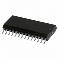
74HCT7030D,112 NXP Semiconductors, 74HCT7030D,112 Datasheet - Page 12

74HCT7030D,112
Manufacturer Part Number
74HCT7030D,112
Description
IC 9X64 FIFO REGISTER 3ST 28SOIC
Manufacturer
NXP Semiconductors
Series
74HCTr
Datasheets
1.74HCT4046ADB112.pdf
(19 pages)
2.74HCT4046ADB112.pdf
(23 pages)
3.74HC7030D652.pdf
(22 pages)
Specifications of 74HCT7030D,112
Function
Asynchronous, Synchronous
Memory Size
576 (9 x 64)
Data Rate
33MHz
Voltage - Supply
4.5 V ~ 5.5 V
Mounting Type
Surface Mount
Package / Case
28-SOIC (7.5mm Width)
Logic Family
HCT
Logical Function
FIFO Register
Number Of Elements
1
Number Of Bits
9
Number Of Inputs
9
Number Of Outputs
9
High Level Output Current
-6mA
Low Level Output Current
6mA
Propagation Delay Time
117ns
Operating Supply Voltage (typ)
5V
Operating Supply Voltage (max)
5.5V
Operating Supply Voltage (min)
4.5V
Output Type
3-State
Polarity
Non-Inverting
Technology
CMOS
Frequency (max)
36(Typ)MHz
Mounting
Surface Mount
Pin Count
28
Operating Temp Range
-40C to 125C
Operating Temperature Classification
Automotive
Quiescent Current
50uA
Lead Free Status / RoHS Status
Lead free / RoHS Compliant
Operating Temperature
-
Access Time
-
Lead Free Status / Rohs Status
Compliant
Other names
568-2900-5
933798900112
933798900112
Philips Semiconductors
AC WAVEFORMS
Shifting in sequence FIFO empty to FIFO full
With FIFO full; SI held HIGH in anticipation of empty location
December 1990
9-bit x 64-word FIFO register; 3-state
(1) HC : V
Fig.6
(1) HC : V
Fig.7
HCT: V
HCT: V
Waveforms showing the SI input to DIR output propagation
delay. The SI pulse width and SI maximum pulse frequency.
Waveforms showing bubble-up delay, SO input to DIR output
and DIR output pulse width.
M
M
M
M
= 50%; V
= 50%; V
= 1.3 V; V
= 1.3 V; V
I
I
I
I
= GND to V
= GND to V
= GND to 3 V.
= GND to 3 V.
CC
CC
.
.
12
Notes to Fig.6
1. DIR initially HIGH; FIFO is
2. SI set HIGH; data loaded into
3. DIR drops LOW, input stage
4. SI set LOW; data from first
5. DIR goes HIGH, status flag
6. Repeat process to load 2nd word
7. DIR remains LOW; with attempt
Notes to Fig.7
1. FIFO is initially full, shift-in is held
2. SO pulse; data in the output
3. DIR HIGH; when empty location
4. DIR returns to LOW; FIFO is full
5. SI brought LOW; necessary to
prepared for valid data.
input stage.
“busy”.
location “ripple through”.
indicates FIFO prepared for
additional data.
through to 64th word into FIFO.
to shift into full FIFO, no data
transfer occurs.
HIGH.
stage is unloaded, “bubble-up
process of empty locations
begins”.
reached input stage, flag
indicates FIFO is prepared for
data input.
again.
complete shift-in process, DIR
remains LOW, because FIFO is
full.
74HC/HCT7030
Product specification


