74HCT7030D,112 NXP Semiconductors, 74HCT7030D,112 Datasheet - Page 14
74HCT7030D,112
Manufacturer Part Number
74HCT7030D,112
Description
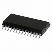
IC 9X64 FIFO REGISTER 3ST 28SOIC
Manufacturer
NXP Semiconductors
Series
74HCTr
Datasheets
1.74HCT4046ADB112.pdf
(19 pages)
2.74HCT4046ADB112.pdf
(23 pages)
3.74HC7030D652.pdf
(22 pages)
Specifications of 74HCT7030D,112
Function
Asynchronous, Synchronous
Memory Size
576 (9 x 64)
Data Rate
33MHz
Voltage - Supply
4.5 V ~ 5.5 V
Mounting Type
Surface Mount
Package / Case
28-SOIC (7.5mm Width)
Logic Family
HCT
Logical Function
FIFO Register
Number Of Elements
1
Number Of Bits
9
Number Of Inputs
9
Number Of Outputs
9
High Level Output Current
-6mA
Low Level Output Current
6mA
Propagation Delay Time
117ns
Operating Supply Voltage (typ)
5V
Operating Supply Voltage (max)
5.5V
Operating Supply Voltage (min)
4.5V
Output Type
3-State
Polarity
Non-Inverting
Technology
CMOS
Frequency (max)
36(Typ)MHz
Mounting
Surface Mount
Pin Count
28
Operating Temp Range
-40C to 125C
Operating Temperature Classification
Automotive
Quiescent Current
50uA
Lead Free Status / RoHS Status
Lead free / RoHS Compliant
Operating Temperature
-
Access Time
-
Lead Free Status / Rohs Status
Compliant
Other names
568-2900-5
933798900112
933798900112


Philips Semiconductors
With FIFO empty; SO is held HIGH in anticipation
Shift-in operation; high-speed burst mode
December 1990
9-bit x 64-word FIFO register; 3-state
(1) HC : V
Fig.10 Waveforms showing ripple through delay SI input to DOR output,
In the high-speed mode, the burst-in rate is determined by the minimum shift-in HIGH and shift-in LOW
specifications. The DIR status flag is a don’t care condition, and a shift-in pulse can be applied regardless of
the flag. A SI pulse which would overflow the storage capacity of the FIFO is ignored.
(1) HC : V
Fig.11 Waveforms showing SI minimum pulse width and SI maximum pulse frequency, in high-speed shift-in
HCT: V
HCT: V
DOR output pulse width and propagation delay from the DOR
pulse to the Q
burst mode.
M
M
M
M
= 50%; V
= 50%; V
= 1.3 V; V
= 1.3 V; V
I
I
I
I
= GND to V
= GND to V
= GND to 3 V.
= GND to 3 V.
n
output.
CC
CC
.
.
14
Notes to Fig.10
1. FIFO is initially empty, SO is held
2. SI pulse; loads data into FIFO
3. DOR flag signals the arrival of
4. Output transition; data arrives at
5. DOR goes LOW; FIFO is empty
6. SO set LOW; necessary to
HIGH.
and initiates ripple through
process.
valid data at the output stage.
output stage after the specified
propagation delay between the
rising edge of the DOR pulse to
the Q
again.
complete shift-out process. DOR
remains LOW, because FIFO is
empty.
n
74HC/HCT7030
output.
Product specification
Related parts for 74HCT7030D,112
Image
Part Number
Description
Manufacturer
Datasheet
Request
R

Part Number:
Description:
9-bit X 64-word Fifo Register; 3-state
Manufacturer:
NXP Semiconductors
Datasheet:
Part Number:
Description:
NXP Semiconductors designed the LPC2420/2460 microcontroller around a 16-bit/32-bitARM7TDMI-S CPU core with real-time debug interfaces that include both JTAG andembedded trace
Manufacturer:
NXP Semiconductors
Datasheet:

Part Number:
Description:
NXP Semiconductors designed the LPC2458 microcontroller around a 16-bit/32-bitARM7TDMI-S CPU core with real-time debug interfaces that include both JTAG andembedded trace
Manufacturer:
NXP Semiconductors
Datasheet:
Part Number:
Description:
NXP Semiconductors designed the LPC2468 microcontroller around a 16-bit/32-bitARM7TDMI-S CPU core with real-time debug interfaces that include both JTAG andembedded trace
Manufacturer:
NXP Semiconductors
Datasheet:
Part Number:
Description:
NXP Semiconductors designed the LPC2470 microcontroller, powered by theARM7TDMI-S core, to be a highly integrated microcontroller for a wide range ofapplications that require advanced communications and high quality graphic displays
Manufacturer:
NXP Semiconductors
Datasheet:
Part Number:
Description:
NXP Semiconductors designed the LPC2478 microcontroller, powered by theARM7TDMI-S core, to be a highly integrated microcontroller for a wide range ofapplications that require advanced communications and high quality graphic displays
Manufacturer:
NXP Semiconductors
Datasheet:
Part Number:
Description:
The Philips Semiconductors XA (eXtended Architecture) family of 16-bit single-chip microcontrollers is powerful enough to easily handle the requirements of high performance embedded applications, yet inexpensive enough to compete in the market for hi
Manufacturer:
NXP Semiconductors
Datasheet:
Part Number:
Description:
The XA-S3 device is a member of Philips Semiconductors? XA(eXtended Architecture) family of high performance 16-bitsingle-chip microcontrollers
Manufacturer:
NXP Semiconductors
Datasheet:

Part Number:
Description:
The NXP BlueStreak LH75401/LH75411 family consists of two low-cost 16/32-bit System-on-Chip (SoC) devices
Manufacturer:
NXP Semiconductors
Datasheet:
Part Number:
Description:
The NXP LPC3130/3131 combine an 180 MHz ARM926EJ-S CPU core, high-speed USB2
Manufacturer:
NXP Semiconductors
Datasheet:
Part Number:
Description:
The NXP LPC3141 combine a 270 MHz ARM926EJ-S CPU core, High-speed USB 2
Manufacturer:
NXP Semiconductors
Part Number:
Description:
The NXP LPC3143 combine a 270 MHz ARM926EJ-S CPU core, High-speed USB 2
Manufacturer:
NXP Semiconductors

Part Number:
Description:
The NXP LPC3152 combines an 180 MHz ARM926EJ-S CPU core, High-speed USB 2
Manufacturer:
NXP Semiconductors
Part Number:
Description:
The NXP LPC3154 combines an 180 MHz ARM926EJ-S CPU core, High-speed USB 2
Manufacturer:
NXP Semiconductors