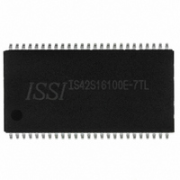
IS42S16100E-7TL ISSI, Integrated Silicon Solution Inc, IS42S16100E-7TL Datasheet - Page 3

IS42S16100E-7TL
Manufacturer Part Number
IS42S16100E-7TL
Description
IC SDRAM 16MBIT 143MHZ 50TSOP
Manufacturer
ISSI, Integrated Silicon Solution Inc
Type
SDRAMr
Specifications of IS42S16100E-7TL
Format - Memory
RAM
Memory Type
SDRAM
Memory Size
16M (1M x 16)
Speed
143MHz
Interface
Parallel
Voltage - Supply
3 V ~ 3.6 V
Operating Temperature
0°C ~ 70°C
Package / Case
50-TSOPII
Organization
1Mx16
Density
16Mb
Address Bus
12b
Access Time (max)
6/5.5ns
Maximum Clock Rate
143MHz
Operating Supply Voltage (typ)
3.3V
Package Type
TSOP-II
Operating Temp Range
0C to 70C
Operating Supply Voltage (max)
3.6V
Operating Supply Voltage (min)
3V
Supply Current
130mA
Pin Count
50
Mounting
Surface Mount
Operating Temperature Classification
Commercial
Lead Free Status / RoHS Status
Lead free / RoHS Compliant
Other names
706-1071
IS42S16100E-7TL
IS42S16100E-7TL
Available stocks
Company
Part Number
Manufacturer
Quantity
Price
Company:
Part Number:
IS42S16100E-7TL
Manufacturer:
ISSI
Quantity:
6 545
Company:
Part Number:
IS42S16100E-7TL
Manufacturer:
ISSI
Quantity:
851
Company:
Part Number:
IS42S16100E-7TLI
Manufacturer:
ISSI
Quantity:
11 200
Company:
Part Number:
IS42S16100E-7TLI
Manufacturer:
ISSI
Quantity:
104
Part Number:
IS42S16100E-7TLI
Manufacturer:
ISSI
Quantity:
20 000
IS42S16100E, IC42S16100E
PIN FUNCTIONS
Integrated Silicon Solution, Inc. — www.issi.com
Rev. C
01/22/08
12, 39, 40, 42, 43,
2, 3, 5, 6, 8, 9, 11
45, 46, 48, 49
7, 13, 38, 44
4, 10, 41, 47
Pin No.
20 to 24
27 to 32
14, 36
26, 50
1, 25
19
16
34
35
18
17
15
Symbol
A0-A10
DQ0 to
LDQM,
UDQM
GNdQ
VddQ
DQ15
GNd
CAS
CKE
RAS
Vdd
CLK
A11
CS
WE
Power Supply Pin
Power Supply Pin
Power Supply Pin
Power Supply Pin
Input Pin
Input Pin
Input Pin
Input Pin
Input Pin
Input Pin
Input Pin
Input Pin
Input Pin
DQ Pin
Type
Function (In Detail)
A0 to A10 are address inputs. A0-A10 are used as row address inputs during active
command input and A0-A7 as column address inputs during read or write command input.
A10 is also used to determine the precharge mode during other commands. If A10 is
LOW during precharge command, the bank selected by A11 is precharged, but if A10 is
HIGH, both banks will be precharged.
When A10 is HIGH in read or write command cycle, the precharge starts automatically
after the burst access.
These signals become part of the OP CODE during mode register set command input.
A11 is the bank selection signal. When A11 is LOW, bank 0 is selected and when high,
bank 1 is selected. This signal becomes part of the OP CODE during mode register set
command input.
CAS, in conjunction with the RAS and WE, forms the device command. See the
“Command Truth Table” item for details on device commands.
The CKE input determines whether the CLK input is enabled within the device. When is
CKE HIGH, the next rising edge of the CLK signal will be valid, and when LOW, invalid.
When CKE is LOW, the device will be in either the power-down mode, the clock suspend
mode, or the self refresh mode. The CKE is an asynchronous input.
CLK is the master clock input for this device. Except for CKE, all inputs to this device are
acquired in synchronization with the rising edge of this pin.
The CS input determines whether command input is enabled within the device.
Command input is enabled when CS is LOW, and disabled with CS is HIGH. The device
remains in the previous state when CS is HIGH.
DQ0 to DQ15 are DQ pins. DQ through these pins can be controlled in byte units
using the LDQM and UDQM pins.
LDQM and UDQM control the lower and upper bytes of the DQ buffers. In read
mode, LDQM and UDQM control the output buffer. When LDQM or UDQM is LOW, the
corresponding buffer byte is enabled, and when HIGH, disabled. The outputs go
the HIGH impedance state when LDQM/UDQM is HIGH. This function corresponds to OE
in conventional DRAMs. In write mode, LDQM and UDQM control the input buffer. When
LDQM or UDQM is LOW, the corresponding buffer byte is enabled, and data can be
written to the device. When LDQM or UDQM is HIGH, input data is masked and cannot
be written to the device.
RAS, in conjunction with CAS and WE, forms the device command. See the “Command
Truth Table” item for details on device commands.
Truth Table” item for details on device commands.
VddQ is the output buffer power supply.
Vdd is the device internal power supply.
GNdQ is the output buffer ground.
GNd is the device internal ground.
WE, in conjunction with RAS and CAS, forms the device command. See the “Command
to
3


