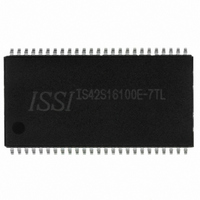
IS42S16100E-7TL ISSI, Integrated Silicon Solution Inc, IS42S16100E-7TL Datasheet - Page 30

IS42S16100E-7TL
Manufacturer Part Number
IS42S16100E-7TL
Description
IC SDRAM 16MBIT 143MHZ 50TSOP
Manufacturer
ISSI, Integrated Silicon Solution Inc
Type
SDRAMr
Specifications of IS42S16100E-7TL
Format - Memory
RAM
Memory Type
SDRAM
Memory Size
16M (1M x 16)
Speed
143MHz
Interface
Parallel
Voltage - Supply
3 V ~ 3.6 V
Operating Temperature
0°C ~ 70°C
Package / Case
50-TSOPII
Organization
1Mx16
Density
16Mb
Address Bus
12b
Access Time (max)
6/5.5ns
Maximum Clock Rate
143MHz
Operating Supply Voltage (typ)
3.3V
Package Type
TSOP-II
Operating Temp Range
0C to 70C
Operating Supply Voltage (max)
3.6V
Operating Supply Voltage (min)
3V
Supply Current
130mA
Pin Count
50
Mounting
Surface Mount
Operating Temperature Classification
Commercial
Lead Free Status / RoHS Status
Lead free / RoHS Compliant
Other names
706-1071
IS42S16100E-7TL
IS42S16100E-7TL
Available stocks
Company
Part Number
Manufacturer
Quantity
Price
Company:
Part Number:
IS42S16100E-7TL
Manufacturer:
ISSI
Quantity:
6 545
Company:
Part Number:
IS42S16100E-7TL
Manufacturer:
ISSI
Quantity:
851
Company:
Part Number:
IS42S16100E-7TLI
Manufacturer:
ISSI
Quantity:
11 200
Company:
Part Number:
IS42S16100E-7TLI
Manufacturer:
ISSI
Quantity:
104
Part Number:
IS42S16100E-7TLI
Manufacturer:
ISSI
Quantity:
20 000
IS42S16100E, IC42S16100E
30
Interval Between Read and Write Commands
A read command can be interrupted and a new write
command executed while the read cycle is in progress,
i.e., before that cycle completes. Data corresponding
to the new write command can be input at the point
new write command is executed. To prevent collision
between input and output data at the DQn pins during
this operation, the
CAS latency = 2, 3, burstlength = 4
COMMAND
U/LDQM
CLK
DQ
READ (CA=A, BANK 0)
READ A0
HI-Z
D
WRITE B0
IN
t
CCD
B0
WRITE (CA=B, BANK 0)
D
IN
B1
D
output data must be masked using the U/LDQM pins. The
interval (t
one clock cycle.
The selected bank must be set to the active state before
executing this command.
IN
B2
Integrated Silicon Solution, Inc. — www.issi.com
ccd
D
IN
) between these commands must be at least
B3
01/22/08
Rev. C


