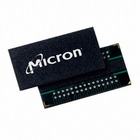
MT41J64M16LA-187E:B TR Micron Technology Inc, MT41J64M16LA-187E:B TR Datasheet - Page 129

MT41J64M16LA-187E:B TR
Manufacturer Part Number
MT41J64M16LA-187E:B TR
Description
IC DDR3 SDRAM 1GBIT 96FBGA
Manufacturer
Micron Technology Inc
Type
DDR3 SDRAMr
Specifications of MT41J64M16LA-187E:B TR
Format - Memory
RAM
Memory Type
DDR3 SDRAM
Memory Size
1G (64M x 16)
Speed
533MHz
Interface
Parallel
Voltage - Supply
1.425 V ~ 1.575 V
Operating Temperature
0°C ~ 95°C
Package / Case
96-FBGA
Organization
64Mx16
Density
1Gb
Address Bus
16b
Maximum Clock Rate
1.066GHz
Operating Supply Voltage (typ)
1.5V
Package Type
FBGA
Operating Temp Range
0C to 95C
Operating Supply Voltage (max)
1.575V
Operating Supply Voltage (min)
1.425V
Supply Current
265mA
Pin Count
96
Mounting
Surface Mount
Operating Temperature Classification
Commercial
Lead Free Status / RoHS Status
Lead free / RoHS Compliant
Other names
557-1378-2
- Current page: 129 of 181
- Download datasheet (9Mb)
READ
Figure 69: READ Latency
PDF: 09005aef826aa906/Source: 09005aef82a357c3
1Gb_DDR3_4.fm - Rev. F 11/08 EN
DQS, DQS#
Command
Address
CK#
DQ
CK
Bank a,
READ
Col n
T0
Notes:
CL = 8, AL = 0
READ bursts are initiated with a READ command. The starting column and bank
addresses are provided with the READ command and auto precharge is either enabled
or disabled for that burst access. If auto precharge is enabled, the row being accessed is
automatically precharged at the completion of the burst. If auto precharge is disabled,
the row will be left open after the completion of the burst.
During READ bursts, the valid data-out element from the starting column address is
available READ latency (RL) clocks later. RL is defined as the sum of POSTED CAS ADDI-
TIVE latency (AL) and CAS latency (CL) (RL = AL + CL). The value of AL and CL is
programmable in the mode register via the MRS command. Each subsequent data-out
element will be valid nominally at the next positive or negative clock edge (that is, at the
next crossing of CK and CK#). Figure 69 shows an example of RL based on a CL setting of
8 and an AL setting of 0.
1. DO n = data-out from column n.
2. Subsequent elements of data-out appear in the programmed order following DO n.
DQS, DQS# is driven by the DRAM along with the output data. The initial low state on
DQS and HIGH state on DQS# is known as the READ preamble (
DQS and the HIGH state on DQS#, coincident with the last data-out element, is known
as the READ postamble (
commands have been initiated, the DQ will go High-Z. A detailed explanation of
(valid data-out skew),
depicted in Figure 80 on page 137. A detailed explanation of
skew to CK) is also depicted in Figure 80 on page 137.
Data from any READ burst may be concatenated with data from a subsequent READ
command to provide a continuous flow of data. The first data element from the new
burst follows the last element of a completed burst. The new READ command should be
issued
page 131. If BC4 is enabled,
output, as shown in Figure 71 on page 131. Nonconsecutive read data is reflected in
Figure 72 on page 132. DDR3 SDRAM do not allow interrupting or truncating any READ
burst.
NOP
T7
t
CCD cycles after the first READ command. This is shown for BL8 in Figure 70 on
NOP
T8
DO
n
t
QH (data-out window hold), and the valid data window are
t
RPST). Upon completion of a burst, assuming no other
NOP
T9
t
CCD must still be met which will cause a gap in the data
129
NOP
T10
Micron Technology, Inc., reserves the right to change products or specifications without notice.
Indicates A Break in
Time Scale
1Gb: x4, x8, x16 DDR3 SDRAM
NOP
T11
Transitioning Data
t
DQSCK (DQS transition
©2006 Micron Technology, Inc. All rights reserved.
t
T12
NOP
RPRE). The low state on
Operations
NOP
T12
Don’t Care
t
DQSQ
Related parts for MT41J64M16LA-187E:B TR
Image
Part Number
Description
Manufacturer
Datasheet
Request
R

Part Number:
Description:
IC DDR3 SDRAM 1GBIT 96FBGA
Manufacturer:
Micron Technology Inc
Datasheet:

Part Number:
Description:
Manufacturer:
Micron Technology Inc
Datasheet:

Part Number:
Description:
Manufacturer:
Micron Technology Inc
Datasheet:

Part Number:
Description:
Manufacturer:
Micron Technology Inc
Datasheet:

Part Number:
Description:
IC SDRAM 64MBIT 133MHZ 54TSOP
Manufacturer:
Micron Technology Inc
Datasheet:

Part Number:
Description:
IC SDRAM 64MBIT 5.5NS 86TSOP
Manufacturer:
Micron Technology Inc
Datasheet:

Part Number:
Description:
IC SDRAM 64MBIT 200MHZ 86TSOP
Manufacturer:
Micron Technology Inc
Datasheet:

Part Number:
Description:
IC SDRAM 64MBIT 133MHZ 54TSOP
Manufacturer:
Micron Technology Inc
Datasheet:

Part Number:
Description:
IC SDRAM 128MBIT 133MHZ 54TSOP
Manufacturer:
Micron Technology Inc
Datasheet:

Part Number:
Description:
IC SDRAM 256MBIT 133MHZ 90VFBGA
Manufacturer:
Micron Technology Inc
Datasheet:

Part Number:
Description:
IC SDRAM 128MBIT 133MHZ 54TSOP
Manufacturer:
Micron Technology Inc
Datasheet:

Part Number:
Description:
IC SDRAM 256MBIT 133MHZ 54TSOP
Manufacturer:
Micron Technology Inc
Datasheet:

Part Number:
Description:
IC DDR SDRAM 512MBIT 6NS 66TSOP
Manufacturer:
Micron Technology Inc
Datasheet:

Part Number:
Description:
IC SDRAM 128MBIT 167MHZ 86TSOP
Manufacturer:
Micron Technology Inc
Datasheet:

Part Number:
Description:
IC SDRAM 128MBIT 143MHZ 86TSOP
Manufacturer:
Micron Technology Inc
Datasheet:


