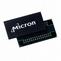
MT41J64M16LA-187E:B TR Micron Technology Inc, MT41J64M16LA-187E:B TR Datasheet - Page 167

MT41J64M16LA-187E:B TR
Manufacturer Part Number
MT41J64M16LA-187E:B TR
Description
IC DDR3 SDRAM 1GBIT 96FBGA
Manufacturer
Micron Technology Inc
Type
DDR3 SDRAMr
Specifications of MT41J64M16LA-187E:B TR
Format - Memory
RAM
Memory Type
DDR3 SDRAM
Memory Size
1G (64M x 16)
Speed
533MHz
Interface
Parallel
Voltage - Supply
1.425 V ~ 1.575 V
Operating Temperature
0°C ~ 95°C
Package / Case
96-FBGA
Organization
64Mx16
Density
1Gb
Address Bus
16b
Maximum Clock Rate
1.066GHz
Operating Supply Voltage (typ)
1.5V
Package Type
FBGA
Operating Temp Range
0C to 95C
Operating Supply Voltage (max)
1.575V
Operating Supply Voltage (min)
1.425V
Supply Current
265mA
Pin Count
96
Mounting
Surface Mount
Operating Temperature Classification
Commercial
Lead Free Status / RoHS Status
Lead free / RoHS Compliant
Other names
557-1378-2
- Current page: 167 of 181
- Download datasheet (9Mb)
Synchronous ODT Mode
ODT Latency and Posted ODT
Timing Parameters
PDF: 09005aef826aa906/Source: 09005aef82a357c3
1Gb_DDR3_5.fm - Rev. F 11/08 EN
Synchronous ODT mode is selected whenever the DLL is turned on and locked and
when either R
modes are:
• Any bank active with CKE HIGH
• Refresh mode with CKE HIGH
• Idle mode with CKE HIGH
• Active power-down mode (regardless of MR0[12])
• Precharge power-down mode if DLL is enabled during precharge power-down by
In synchronous ODT mode, R
HIGH by a rising clock edge and turns off ODTL off clock cycles after ODT is registered
LOW by a rising clock edge. The actual on/off times varies by
each clock edge (see Table 81 on page 168). The ODT latency is tied to the WRITE latency
(WL) by ODTL on = WL - 2 and ODTL off = WL - 2.
Since write latency is made up of CAS WRITE latency (CWL) and ADDITIVE latency (AL),
the AL programmed into the mode register (MR1[4, 3]) also applies to the ODT signal.
The DRAM’s internal ODT signal is delayed a number of clock cycles defined by the AL
relative to the external ODT signal. Thus ODTL on = CWL + AL - 2 and ODTL
off = CWL + AL - 2.
Synchronous ODT mode uses the following timing parameters: ODTL on, ODTL off,
ODTH4, ODTH8
minimum R
and ODT resistance begins to turn on. Maximum R
point at which ODT resistance is fully on. Both are measured relative to ODTL on. The
minimum R
off ODT resistance. Maximum R
has reached High-Z. Both are measured from ODTL off.
When ODT is asserted, it must remain HIGH until ODTH4 is satisfied. If a WRITE
command is registered by the DRAM with ODT HIGH, then ODT must remain HIGH
until ODTH4 (BC4) or ODTH8 (BL8) after the WRITE command (see Figure 117 on
page 169). ODTH4 and ODTH8 are measured from ODT registered HIGH to ODT regis-
tered LOW or from the registration of a WRITE command until ODT is registered LOW.
MR0[12]
TT
TT
TT
turn-on time (
turn-off time (
_
,
NOM
t
AON, and
or R
TT
_
t
167
t
t
AOF (see Table 81 and Figure 116 on page 168). The
WR
AON [MIN]) is the point at which the device leaves High-Z
TT
AOF [MIN]) is the point at which the device starts to turn
TT
turns on ODTL on clock cycles after ODT is sampled
is enabled. Based on the power-down definition, these
turn off time (
Micron Technology, Inc., reserves the right to change products or specifications without notice.
1Gb: x4, x8, x16 DDR3 SDRAM
t
AOF [MAX]) is the point at which ODT
TT
turn-on time (
On-Die Termination (ODT)
t
AON and
©2006 Micron Technology, Inc. All rights reserved.
t
AON [MAX]) is the
t
AOF around
Related parts for MT41J64M16LA-187E:B TR
Image
Part Number
Description
Manufacturer
Datasheet
Request
R

Part Number:
Description:
IC DDR3 SDRAM 1GBIT 96FBGA
Manufacturer:
Micron Technology Inc
Datasheet:

Part Number:
Description:
Manufacturer:
Micron Technology Inc
Datasheet:

Part Number:
Description:
Manufacturer:
Micron Technology Inc
Datasheet:

Part Number:
Description:
Manufacturer:
Micron Technology Inc
Datasheet:

Part Number:
Description:
IC SDRAM 64MBIT 133MHZ 54TSOP
Manufacturer:
Micron Technology Inc
Datasheet:

Part Number:
Description:
IC SDRAM 64MBIT 5.5NS 86TSOP
Manufacturer:
Micron Technology Inc
Datasheet:

Part Number:
Description:
IC SDRAM 64MBIT 200MHZ 86TSOP
Manufacturer:
Micron Technology Inc
Datasheet:

Part Number:
Description:
IC SDRAM 64MBIT 133MHZ 54TSOP
Manufacturer:
Micron Technology Inc
Datasheet:

Part Number:
Description:
IC SDRAM 128MBIT 133MHZ 54TSOP
Manufacturer:
Micron Technology Inc
Datasheet:

Part Number:
Description:
IC SDRAM 256MBIT 133MHZ 90VFBGA
Manufacturer:
Micron Technology Inc
Datasheet:

Part Number:
Description:
IC SDRAM 128MBIT 133MHZ 54TSOP
Manufacturer:
Micron Technology Inc
Datasheet:

Part Number:
Description:
IC SDRAM 256MBIT 133MHZ 54TSOP
Manufacturer:
Micron Technology Inc
Datasheet:

Part Number:
Description:
IC DDR SDRAM 512MBIT 6NS 66TSOP
Manufacturer:
Micron Technology Inc
Datasheet:

Part Number:
Description:
IC SDRAM 128MBIT 167MHZ 86TSOP
Manufacturer:
Micron Technology Inc
Datasheet:

Part Number:
Description:
IC SDRAM 128MBIT 143MHZ 86TSOP
Manufacturer:
Micron Technology Inc
Datasheet:


