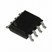
FAN102MY Fairchild Semiconductor, FAN102MY Datasheet - Page 4

FAN102MY
Manufacturer Part Number
FAN102MY
Description
IC CTRLR PWM GREEN CV/CC 8SOP
Manufacturer
Fairchild Semiconductor
Datasheet
1.FAN102MY.pdf
(16 pages)
Specifications of FAN102MY
Output Isolation
Isolated
Frequency Range
39 ~ 45kHz
Voltage - Input
5.5 ~ 15 V
Voltage - Output
30V
Power (watts)
660mW
Operating Temperature
-40°C ~ 105°C
Package / Case
8-SOIC (0.154", 3.90mm Width)
Number Of Outputs
1
Duty Cycle (max)
75 %
Mounting Style
SMD/SMT
Switching Frequency
45 KHz
Maximum Operating Temperature
+ 105 C
Fall Time
80 ns
Minimum Operating Temperature
- 40 C
Rise Time
200 ns
Synchronous Pin
No
Topology
Flyback
Lead Free Status / RoHS Status
Lead free / RoHS Compliant
Other names
FAN102MYTR
Available stocks
Company
Part Number
Manufacturer
Quantity
Price
© 2008 Fairchild Semiconductor Corporation
FAN102 Rev. 1.0.3
Absolute Maximum Ratings
Stresses exceeding the absolute maximum ratings may damage the device. The device may not function or be
operable above the recommended operating conditions and stressing the parts to these levels is not recommended.
In addition, extended exposure to stresses above the recommended operating conditions may affect device reliability.
The absolute maximum ratings are stress ratings only.
Notes:
1.
2.
Recommended Operating Conditions
The Recommended Operating Conditions table defines the conditions for actual device operation. Recommended
operating conditions are specified to ensure optimal performance to the datasheet specifications. Fairchild does not
recommend exceeding them or designing to Absolute Maximum Ratings.
Symbol
T
Symbol
Stresses beyond those listed under ”absolute maximum ratings” may cause permanent damage to the device.
All voltage values, except differential voltages, are given with respect to GND pin.
A
V
V
ESD
T
V
V
V
Θ
Θ
COMV
P
COMI
T
T
STG
DD
CS
VS
JA
JC
D
J
L
Operating Ambient Temperature
DC Supply Voltage
VS Pin Input Voltage
CS Pin Input Voltage
Voltage Error Amplifier Output Voltage
Voltage Error Amplifier Output Voltage
Power Dissipation (T
Thermal Resistance (Junction-to-Air)
Thermal Resistance (Junction-to-Case)
Operating Junction Temperature
Storage Temperature Range
Lead Temperature (Wave Soldering or IR, 10 Seconds)
Electrostatic Discharge Capability,
Human Body Model, JEDEC- JESD22_A114
Electrostatic Discharge Capability,
Charged Device Model, JEDEC- JESD22_C101
Parameter
(1,2)
A
Parameter
<50°C)
Conditions
4
Min.
-40
Min.
Typ.
-0.3
-0.3
-0.3
-0.3
-55
Max.
+150
+150
+260
1250
Max.
+105
660
150
7.0
7.0
7.0
7.0
4.5
30
39
www.fairchildsemi.com
°C /W
°C /W
Unit
Unit
mW
kV
°C
°C
°C
°C
V
V
V
V
V
V


