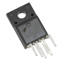
FSQ0765RQUDTU Fairchild Semiconductor, FSQ0765RQUDTU Datasheet - Page 17

FSQ0765RQUDTU
Manufacturer Part Number
FSQ0765RQUDTU
Description
IC CONV QUASI-RES 650V TO-220F-6
Manufacturer
Fairchild Semiconductor
Series
FPS™r
Datasheet
1.FSQ0765RQWDTU.pdf
(19 pages)
Specifications of FSQ0765RQUDTU
Output Isolation
Isolated
Frequency Range
48kHz ~ 67kHz
Voltage - Input
9 V ~ 20 V
Voltage - Output
650V
Power (watts)
90W
Operating Temperature
-25°C ~ 85°C
Package / Case
TO-220-6 Formed Leads
On Resistance (max)
1.3 Ohms
Maximum Operating Temperature
+ 85 C
Minimum Operating Temperature
+ 25 C
Maximum Power Dissipation
45 W
Mounting Style
Through Hole
Off Time (max)
63 ns
On Time (max)
27 ns
Operating Frequency
66.7 KHz
Propagation Delay Time
200 ns
Supply Current
3 mA
Supply Voltage (max)
20 V
Lead Free Status / RoHS Status
Lead free / RoHS Compliant
Available stocks
Company
Part Number
Manufacturer
Quantity
Price
Company:
Part Number:
FSQ0765RQUDTU
Manufacturer:
Fairchi/ON
Quantity:
30 000
PCB Layout Guide
Due to the combined scheme, FPS shows better noise
immunity than conventional PWM
controller and
MOSFET discrete solution. Further more are internal
drain current sense eliminates the possibility of noise
generation caused by a sensing resistor. There are some
recommendations for PCB layout to enhance noise
immunity and suppress natural noise inevitable in power-
handling components.
There are typically two grounds in the conventional
SMPS: power ground and signal ground. The power
ground is the ground for primary input voltage and
power, while the signal ground is ground for PWM
controller. In FPS, those two grounds share the same
pin, GND. Normally the separate grounds do not share
the same trace and meet only at one point, the GND pin.
More, wider patterns for both grounds are good for large
currents by decreasing resistance.
Capacitors at the VCC and FB pins should be as close
as possible to the corresponding pins to avoid noise from
the switching device. Sometimes Mylar® or ceramic
capacitors with electrolytic for V
are better for smooth
CC
operation. The ground of these capacitors needs to
Figure 37. Recommended PCB Layout
connect to the signal ground (not power ground).
The cathode of the snubber diode should be close to the
drain pin to minimize stray inductance. The Y-capacitor
between primary and secondary should be directly
connected to the power ground of DC link to maximize
surge immunity.
Because the voltage range of feedback and sync line is
small, it is affected by the noise of the drain pin. Those
traces should not draw across or close to the drain line.
When the heat sink is connected to the ground, it should
be connected to the power ground. If possible, avoid
using jumper wires for power ground and drain.
Mylar® is a registered trademark of DuPont Teijin Films.
© 2008 Fairchild Semiconductor Corporation
www.fairchildsemi.com
FSQ0765RQ Rev. 1.0.1
17


