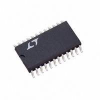
LTC1421CSW#TR Linear Technology, LTC1421CSW#TR Datasheet - Page 12

LTC1421CSW#TR
Manufacturer Part Number
LTC1421CSW#TR
Description
IC CONTROLLER HOTSWAP ADJ 24SOIC
Manufacturer
Linear Technology
Type
Hot-Swap Controllerr
Datasheet
1.LTC1421CG-2.5PBF.pdf
(24 pages)
Specifications of LTC1421CSW#TR
Applications
General Purpose
Internal Switch(s)
No
Voltage - Supply
3 V ~ 12 V
Operating Temperature
0°C ~ 70°C
Mounting Type
Surface Mount
Package / Case
24-SOIC (0.300", 7.50mm Width)
Linear Misc Type
Positive Low Voltage
Family Name
LTC1421
Package Type
SOIC W
Operating Supply Voltage (min)
3V
Operating Supply Voltage (max)
12V
Operating Temperature (min)
0C
Operating Temperature (max)
70C
Operating Temperature Classification
Commercial
Mounting
Surface Mount
Pin Count
24
Lead Free Status / RoHS Status
Contains lead / RoHS non-compliant
Lead Free Status / RoHS Status
Contains lead / RoHS non-compliant
Available stocks
Company
Part Number
Manufacturer
Quantity
Price
APPLICATIONS
LTC1421/LTC1421-2.5
When V
the 1 F capacitor connected to AUXV
discharge circuitry alive long enough to fully turn off the
external N-channels.
Power N-Channel Selection
The R
enough so that the voltage drop across it is about 200mV
or less at full current. If the R
drop across the transistor might cause the output voltage
to trip the reset circuit. Table 2 lists the transistors that are
recommended for use with the LTC1421.
Table 2. N-Channel Selection Guide
CURRENT
LEVEL (A)
0 to 1
1 to 2
2 to 5
5 to 10
10 to 20
Data Bus
When a board is inserted or removed from the host, care
must be given to prevent the system data bus from being
corrupted when the data pins make or break contact. One
problem is that the fully discharged input or output capaci-
tance of the logic gates on the board will draw an inrush
current when the data bus pins first make contact. The
inrush current can temporarily corrupt the data bus, but
usually will not cause long term damage. The problem can
be minimized by insuring the input or output data bus
capacitance is kept as small as possible.
The second, and more serious problem involves the
diodes to V
(Figure 12).
12
DS(ON)
CCLO
MMDF3NO2HD ON Semiconductor
MTB75N05HD
CC
MMDF2N02E
MTB50N06E
MTB30N06
NUMBER
collapses, there is enough energy stored on
of the external pass transistor must be low
at the input and output of most logic families
PART
U
ON Semiconductor
ON Semiconductor
ON Semiconductor
ON Semiconductor
MANUFACTURER
INFORMATION
U
DS(ON)
is too high, the voltage
W
CC
DESCRIPTION
Dual N-Channel SO-8
R
Dual N-Channel SO-8
R
Single 30A
N-Channel DD Pak
R
Single
N-Channel DD Pak
R
Single
N-Channel DD Pak
R
to keep the gate
DS(ON)
DS(ON)
DS(ON)
DS(ON)
DS(ON)
U
= 0.1
= 0.09
= 0.05
= 0.025
= 0.0095
With the board initially unpowered, the V
logic gate is at ground potential. When the data bus pins
make contact, the bus line is clamped to ground through
the input diode D1 to V
flow through the diode and cause the logic gate to latch up
and destroy itself when the power is finally applied. This
DATA BUS
SYSTEM
Figure 12. Typical Logic Gate Loading the Data Bus
5V
BACKPLANE
DATA
BUS
Figure 13: Buffering the Data Bus
15
16
19
20
10
23
13
2
5
6
9
1
5
DISABLE
3
1
23
CC
0.005
QS3384
. Large amounts of current can
R1
BOARD
D1
D2
LTC1421
2
4
22
MTB50N06E
GND
V
V
CC
CC
Q1
21 20
24
3
14
4
17
7
18
8
21
11
22
12
GND
12
1421 F13
OUT
CC
+
1421 F12
BOARD
DATA BUS
input to the
C
LOAD
V
CC


