LTC1421CSW#TR Linear Technology, LTC1421CSW#TR Datasheet - Page 18

LTC1421CSW#TR
Manufacturer Part Number
LTC1421CSW#TR
Description
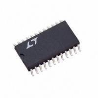
IC CONTROLLER HOTSWAP ADJ 24SOIC
Manufacturer
Linear Technology
Type
Hot-Swap Controllerr
Datasheet
1.LTC1421CG-2.5PBF.pdf
(24 pages)
Specifications of LTC1421CSW#TR
Applications
General Purpose
Internal Switch(s)
No
Voltage - Supply
3 V ~ 12 V
Operating Temperature
0°C ~ 70°C
Mounting Type
Surface Mount
Package / Case
24-SOIC (0.300", 7.50mm Width)
Linear Misc Type
Positive Low Voltage
Family Name
LTC1421
Package Type
SOIC W
Operating Supply Voltage (min)
3V
Operating Supply Voltage (max)
12V
Operating Temperature (min)
0C
Operating Temperature (max)
70C
Operating Temperature Classification
Commercial
Mounting
Surface Mount
Pin Count
24
Lead Free Status / RoHS Status
Contains lead / RoHS non-compliant
Lead Free Status / RoHS Status
Contains lead / RoHS non-compliant
Available stocks
Company
Part Number
Manufacturer
Quantity
Price
module. The ground pin for the LTC1421 is connected to
– 48V; Zener diode D1 and resistor R1 provide the positive
supply for the chip. Bypass capacitor C4 is protected
against inrush current by P-channel Q1. When the board
is inserted into the backplane, transistor Q1 is turned off
by resistor R2. When the connection sense pins, CON1
and CON2 have been connected to – 48V for more than
20ms, CPON pulls high turning on Q2 and the gate of Q1
starts to pull low with a time constant determined by R2,
R3 and C3. At the same time, the voltage at the input to the
power module starts to ramp up. When the voltage across
the inputs to the power module reaches the comparator
trip level set by R5 and R6, in this case – 32V, the
comparator output pulls high and turns on the 5V supply.
A cheaper solution is shown in Figure 20 using the
LT
tects the bypass capacitors against inrush current and
resistors R5 and R6 set the comparator trip voltage. The
LT1170HV is turned on via the V
and transistor Q4 provide a monitoring path for the RESET
signal which is level shifted up to 5V through an optoiso-
lator.
The P-channel power FET is being replaced by an
N-channel FET in Figure 21 for the – 48V application.
Again, Zener Diode D1 and resistor R1 provide the positive
supply for the chip. Capacitor C1 is to insure Q1 stays off
when the board is being hot inserted into the backplane.
The resistor divider R2 and R3, along with the internal
comparator, perform the undervoltage lock out function.
Q1 would only be turned on when the input supply voltage
is lower than – 42V. The power module would then be
turned on by the optoisolator, 4N25, when the module’s
input voltage reaches 47V.
Figure 22 shows how to use the LTC1421 with a 24V
supply and a LT1074CT step-down switcher. Resistors R5
and R6 set the turn-on threshold to 22V. All of the
supervisory signals can be used without level shifting.
LTC1421/LTC1421-2.5
18
APPLICATIONS
®
1170HV switcher. Again P-channel transistor Q1 pro-
U
INFORMATION
U
C
pin. Resistors R11, R14
W
U
Figure 23 shows how to use the LTC1421 with a 5V supply
and an LTC1430CS8 synchronous step-down switching
regulator to generate 3.3V output at up to 10A for micro-
processors. Resistors R4, R8 and R9 set the turn-on
voltage at 4.8V and the turn-off at 4.25V. Pushbutton
switch S1 provides users a way to reset the output while
S2 is used to soft-reset the microprocessor only.
Figure 24 shows how to use the LTC1421 with a 5V supply
and a – 48V supply that is used to generate a 12V supply
using a supply module. Resistors R3 and R4 are used to
monitor the input voltage to the supply module. The
module is prevented from turning on via the optoisolator
until the input voltage reaches – 36V. Zener diode D2
prevents the CPON pin of the LTC1421 from being dam-
aged by excessive voltage.
Figure 25 shows how to use the LTC1421 to do overvolt-
age protection. Resistors R3 and R4 set the trip point at
7V. When the input supply voltage rises above 7V, Q2 is
turned on and Q1 turned off while Q3 helps to discharge
the output voltage.
Figure 26 shows how to use the LTC1421 to control both
the power-up and power-down sequence of the outputs.
The 5V output would be powered up first followed by the
3V output. At power-down sequence, the 3V output would
go down first followed by the 5V supply.
Figure 27 shows how to use the LTC1421 to switch 3.3V,
5V, 12V and –12V supplies for PCI application. The ramp-
up rate for 3.3V, 5V and 12V is determined by the ramp
capacitor C2 while the –12V supply is controlled by R7 and
C3. The internal comparator is being used to do the
overcurrent protection for Q4 with the trip point set by
resistors R6 and R8. The –12V supply does not have
overcurrent protection. R10 is used to set the power good
signal trip point at 10V. When the 12V output rises above
10V, the PCI controller gets a power good signal followed
by RESET after 200ms.


