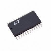
LTC1421CSW#TR Linear Technology, LTC1421CSW#TR Datasheet - Page 6

LTC1421CSW#TR
Manufacturer Part Number
LTC1421CSW#TR
Description
IC CONTROLLER HOTSWAP ADJ 24SOIC
Manufacturer
Linear Technology
Type
Hot-Swap Controllerr
Datasheet
1.LTC1421CG-2.5PBF.pdf
(24 pages)
Specifications of LTC1421CSW#TR
Applications
General Purpose
Internal Switch(s)
No
Voltage - Supply
3 V ~ 12 V
Operating Temperature
0°C ~ 70°C
Mounting Type
Surface Mount
Package / Case
24-SOIC (0.300", 7.50mm Width)
Linear Misc Type
Positive Low Voltage
Family Name
LTC1421
Package Type
SOIC W
Operating Supply Voltage (min)
3V
Operating Supply Voltage (max)
12V
Operating Temperature (min)
0C
Operating Temperature (max)
70C
Operating Temperature Classification
Commercial
Mounting
Surface Mount
Pin Count
24
Lead Free Status / RoHS Status
Contains lead / RoHS non-compliant
Lead Free Status / RoHS Status
Contains lead / RoHS non-compliant
Available stocks
Company
Part Number
Manufacturer
Quantity
Price
PIN
LTC1421/LTC1421-2.5
6
RAMP (Pin 10): Analog Power-Up Ramp Control Pin. By
connecting an external capacitor between the RAMP and
GATEHI, a positive linear voltage ramp on GATEHI and
GATELO is generated on power-up with a slope equal to
20 A/C
enhances the ESD performance at the GATEHI pin.
FB (Pin 11): Analog Feedback Input. FB is used to set the
reset threshold voltage on V
floating. For a 3.3V supply, short FB to V
GND (Pin 12): Ground
COMP + (Pin 13): Noninverting Comparator Input.
COMP – (Pin 14): Inverting Comparator Input.
COMPOUT (Pin 15): Open Drain Comparator Output.
V
the higher of the two supply voltage outputs.
GATEHI (Pin 17): The High Side Gate Drive for the High
Supply N-Channel. An internal charge pump guarantees at
least 6V of gate drive. The slope of the voltage rise at
GATEHI is set by the external capacitor connected between
GATEHI and RAMP. When the circuit breaker trips, GATEHI
is immediately pulled to GND.
SETHI (Pin 18): The Circuit Breaker Set Pin for the High
Supply. With a sense resistor placed in the supply path
between V
the voltage across the resistor exceeds 50mV for more
than 20 s. To disable the circuit breaker, V
should be shorted together.
OUTHI
U
FUNCTIONS
(Pin 16): High Supply Voltage Output. This must be
RAMP
CCHI
U
. A 10k resistor in series with the capacitor
and SETHI, the circuit breaker will trip when
U
CCLO
. For a 5V supply leave FB
CCLO
CCHI
.
and SETHI
V
higher of the two input supply voltages. An undervoltage
lockout circuit disables the chip until the voltage at V
is greater than 2.45V.
V
the lower of the two supply voltage outputs.
GATELO (Pin 21): The High Side Gate Drive for the Low
Supply N-Channel Pass Transistor. An internal charge
pump guarantees at least 10V of gate drive. The slope of
the voltage rise at GATELO is set by the external capacitor
connected between GATEHI and RAMP. When the circuit
breaker trips GATELO is immediately pulled to GND.
SETLO (Pin 22): The Circuit Breaker Set Pin for the Low
Supply. With a sense resistor placed in the supply path
between V
when the voltage across the resistor exceeds 50mV for
more than 20 s. To disable the circuit breaker, V
SETLO should be shorted together.
V
equal to or lower voltage than V
lockout circuit disables the chip until the voltage at V
is greater than 2.45V.
AUXV
GATEHI discharge circuitry. Connect a 1 F capacitor to
ground. AUXV
Schottky diode and series resistor.
CCHI
OUTLO
CCLO
(Pin 19): The Positive Supply Input. This must be the
CC
(Pin 23): The Positive Supply Input. V
(Pin 20): Low Supply Voltage Output. This must be
(Pin 24): The supply input for the GATELO and
CCLO
CC
and SETLO, the circuit breaker will trip
is powered from V
CCHI
CCLO
. An undervoltage
via an internal
CCLO
CCLO
must be
CCLO
CCHI
and


