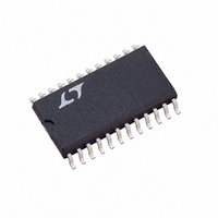
LTC1421CSW#TR Linear Technology, LTC1421CSW#TR Datasheet - Page 14

LTC1421CSW#TR
Manufacturer Part Number
LTC1421CSW#TR
Description
IC CONTROLLER HOTSWAP ADJ 24SOIC
Manufacturer
Linear Technology
Type
Hot-Swap Controllerr
Datasheet
1.LTC1421CG-2.5PBF.pdf
(24 pages)
Specifications of LTC1421CSW#TR
Applications
General Purpose
Internal Switch(s)
No
Voltage - Supply
3 V ~ 12 V
Operating Temperature
0°C ~ 70°C
Mounting Type
Surface Mount
Package / Case
24-SOIC (0.300", 7.50mm Width)
Linear Misc Type
Positive Low Voltage
Family Name
LTC1421
Package Type
SOIC W
Operating Supply Voltage (min)
3V
Operating Supply Voltage (max)
12V
Operating Temperature (min)
0C
Operating Temperature (max)
70C
Operating Temperature Classification
Commercial
Mounting
Surface Mount
Pin Count
24
Lead Free Status / RoHS Status
Contains lead / RoHS non-compliant
Lead Free Status / RoHS Status
Contains lead / RoHS non-compliant
Available stocks
Company
Part Number
Manufacturer
Quantity
Price
LTC1421/LTC1421-2.5
When CON1 and CON2 are both forced to ground for more
than 20ms, the LTC1421 assumes that the board is fully
connected to the host and power-up can begin. When
V
threshold, the 20 A current reference is connected from
RAMP to GND, the charge pumps are turned on and CPON
is forced high (time point 4). V
ramp up. When V
age, PWRGD will immediately be forced high (time point
5). After a 200ms delay, RESET will be pulled high and
DISABLE will be pulled low, enabling the data bus (time
point 6).
Ground Sense Comparator
When POR is pulled low for more than 20ms, GATELO and
GATEHI are pulled to ground and V
be discharged. If POR is pulled back high while V
and V
continue. When they drop below the V
14
APPLICATIONS
CCLO
OUTHI
and V
CCHI
are still ramping down, the discharge will
exceed the 2.45V undervoltage lockout
OUTLO
U
DISABLE
GATELO
PWRGD
GATEHI
V
exceeds the reset threshold volt-
V
RESET
FAULT
V
OUTLO
CPON
V
CON1
CON2
OUTHI
INFORMATION
CCLO
POR
CCHI
U
OUTHI
OUTLO
W
1
and V
TRIP
20ms
and V
point, a power-
OUTLO
Figure 15. Power-On Reset Timing
2
U
OUTHI
V
TH2
begin to
OUTLO
3
will
32 s
4
up sequence will begin automatically. The trip point poten-
tial for LTC1421 is set at 0.1V and 2.5V for LTC1421-2.5.
In applications, where either V
forced above 100mV before power-up, the LTC1421-2.5
should be used. This could occur when leakage through
the body diode of the logic chips keeps V
the case where logic lines are precharged.
In other applications, where outputs need to drop to near
ground potential before ramping up again to ensure proper
initial state for the logic chips, the LTC1421 should be
used.
Power-On Reset Timing
The POR input is used to completely cycle the power
supplies on the board or to reset the electronic circuit
breaker feature. The POR pin can be connected to a
grounded push button, toggle switch or a logic signal
from the host. When POR is pulled low for more than
20ms, a power-on reset sequence begins (Figure 15,
5
6
V
200ms
TH1
7
OUTLO
1421 F15
or V
OUTLO
OUTHI
high or in
might be


