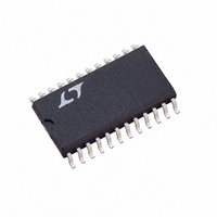
LTC1421CSW#TR Linear Technology, LTC1421CSW#TR Datasheet - Page 5

LTC1421CSW#TR
Manufacturer Part Number
LTC1421CSW#TR
Description
IC CONTROLLER HOTSWAP ADJ 24SOIC
Manufacturer
Linear Technology
Type
Hot-Swap Controllerr
Datasheet
1.LTC1421CG-2.5PBF.pdf
(24 pages)
Specifications of LTC1421CSW#TR
Applications
General Purpose
Internal Switch(s)
No
Voltage - Supply
3 V ~ 12 V
Operating Temperature
0°C ~ 70°C
Mounting Type
Surface Mount
Package / Case
24-SOIC (0.300", 7.50mm Width)
Linear Misc Type
Positive Low Voltage
Family Name
LTC1421
Package Type
SOIC W
Operating Supply Voltage (min)
3V
Operating Supply Voltage (max)
12V
Operating Temperature (min)
0C
Operating Temperature (max)
70C
Operating Temperature Classification
Commercial
Mounting
Surface Mount
Pin Count
24
Lead Free Status / RoHS Status
Contains lead / RoHS non-compliant
Lead Free Status / RoHS Status
Contains lead / RoHS non-compliant
Available stocks
Company
Part Number
Manufacturer
Quantity
Price
TYPICAL PERFORMANCE CHARACTERISTICS
PIN
CON1 (Pin 1): TTL Level Input with a Pull-Up to V
Together with CON2, it is used to indicate board connec-
tion. The pin must be tied to ground on the host side of the
connector. When using staggered connector pins, CON1
and CON2 must be the shortest and must be placed at
opposite corners of the connector. Board insertion is
assumed after CON1 and CON2 are both held low for 20ms
after power-up.
CON2 (Pin 2): TTL Level Input with a Pull-Up to V
Together with CON1 it is used to indicate board connec-
tion.
POR (Pin 3): TTL Level Input with a Pull-Up to V
When the pin is pulled low for at least 20ms, a hard reset
is generated. Both V
controlled rate. A power-up sequence will not start until
the POR pin is pulled high. If POR is pulled high before
V
sequence will not begin until the voltage at V
V
be reset by pulling POR low.
FAULT (Pin 4): Open Drain Output to GND with a Weak
Pull-Up to V
rent fault is detected at V
DISABLE (Pin 5): CMOS Output. The signal is used to
disable the board’s data bus during insertion or removal.
OUTLO
OUTHI
U
FUNCTIONS
are below V
and V
U
CCLO
OUTHI
. The pin is pulled low when an overcur-
5
4
3
2
1
0
TRIP
0
CPON Voltage vs Source Current
(Charge Pump On)
U
OUTLO
are fully discharged, a power-up
. The electronic circuit breaker will
– 0.5
OUTLO
SOURCE CURRENT (mA)
W
and V
– 1.0
or V
U
– 1.5
OUTHI
OUTHI
– 2.0
will turn off at a
V
V
.
CCLO
CCHI
– 2.5
= 12V
= 5V
1421 G10
OUTLO
– 3.0
CCLO
CCLO
CCLO
and
.
.
.
PWRGD (Pin 6): Open Drain Output to GND with a Weak
Pull-Up to V
V
pulled high immediately after V
threshold voltage.
RESET (Pin 7): Open Drain Output to GND with a Weak
Pull-Up to V
condition is detected. A reset will be generated when any
of the following conditions are met: Either CON1 or CON2
is high, POR is pulled low, V
respective undervoltage lockout thresholds, PWRGD goes
low or an overcurrent fault is detected at V
V
high. On power failure, RESET will go low 32 s after
PWRGD goes low.
REF (Pin 8): The Reference Voltage Output. V
1 F bypass capacitor is recommended.
CPON (Pin 9): CMOS Output That Can Be Pulled Below
Ground. CPON is pulled high when the internal charge
pumps for GATELO and GATEHI are turned on. CPON is
pulled low when the charge pumps are turned off. The pin
can be used to control an external MOSFET for a – 5V to
– 12V supply.
OUTLO
OUTHI
1%. The reference can source up to 5mA of current. A
. RESET will go high 200ms after PWRGD goes
falls below its reset threshold voltage. The pin is
7
6
4
3
2
0
5
1
0
I
vs V
CCLO
V
CCLO
CCHI
CCLO
2
CCLO
Supply Current
= 12V
LTC1421/LTC1421-2.5
. The pin is pulled low immediately after
. The pin is pulled low when a reset
Voltage
4
V
CCLO
6
VOLTAGE (V)
8
CCLO
10
OUTLO
or V
12
1421 G11
rises above its reset
CCHI
14
are below their
OUT
OUTLO
= 1.232V
5
or


