MC33982BPNA Freescale Semiconductor, MC33982BPNA Datasheet - Page 12
MC33982BPNA
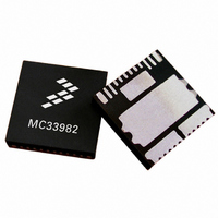
Manufacturer Part Number
MC33982BPNA
Description
IC SWITCH HI SIDE SINGLE 16-PQFN
Manufacturer
Freescale Semiconductor
Type
High Sider
Datasheet
1.MC33982BPNA.pdf
(36 pages)
Specifications of MC33982BPNA
Input Type
SPI
Number Of Outputs
1
On-state Resistance
2 mOhm
Voltage - Supply
6 V ~ 27 V
Operating Temperature
-40°C ~ 125°C
Mounting Type
Surface Mount
Package / Case
16-PQFN, 16-PowerQFN
Lead Free Status / RoHS Status
Contains lead / RoHS non-compliant
Current - Output / Channel
-
Current - Peak Output
-
Available stocks
Company
Part Number
Manufacturer
Quantity
Price

Part Number:
MC33982BPNA
Manufacturer:
FREESCALE
Quantity:
20 000


Table 5. Dynamic Electrical Characteristics (continued)
12
33982
ELECTRICAL CHARACTERISTICS
DYNAMIC ELECTRICAL CHARACTERISTICS
Typical values noted reflect the approximate parameter mean at T
POWER OUTPUT TIMING (CONTINUED)
SPI INTERFACE CHARACTERISTICS
Notes
Over-current Low Detection Blanking Time (OCLT [1:0])
Over-current High Detection Blanking Time
CS to CSNS Valid Time
Output Switching Delay Time (OSD [2:0])
Watchdog Timeout (WD [1:0])
Recommended Frequency of SPI Operation
Required Low-state Duration for RST
23.
24.
25.
Characteristics noted under conditions 4.5 V ≤ V
00
01
10
11
000
001
010
011
100
101
110
111
00
01
10
11
Time necessary for the CSNS to be within ±5% of the targeted value.
Watchdog timeout delay measured from the rising edge of WAKE to RST from a sleep state condition to output turn-ON with the output
driven OFF and FSI floating. The values shown are for WDR setting of [00]. The accuracy of t
watchdog timeouts.
RST
low duration measured with outputs enabled and going to OFF or disabled condition.
(23)
Characteristic
(24)
(25)
DD
≤ 5.5 V, 6.0 V ≤ V
A
= 25°C under nominal conditions, unless otherwise noted.
t
Symbol
t
t
t
t
CNSVAL
t
t
t
t
t
t
t
t
t
t
t
t
t
WDTO0
WDTO1
WDTO2
WDTO3
t
PWR
WRST
OSD0
OSD1
OSD2
OSD3
OSD4
OSD5
OSD6
OSD7
OCL0
OCL1
OCL2
OCL3
f
OCH
SPI
≤ 27 V, -40°C ≤ T
1750
0.08
Min
108
105
157
210
262
315
367
434
207
875
7.0
0.8
1.0
52
–
–
–
–
Analog Integrated Circuit Device Data
WDTO
A
≤ 125°C, unless otherwise noted.
is consistent for all configured
2500
1250
0.15
Typ
155
150
225
300
375
450
525
620
310
1.2
0.0
10
10
75
50
–
–
Freescale Semiconductor
3250
1625
Max
0.25
202
195
293
390
488
585
683
806
403
167
1.6
3.0
13
20
10
95
–
MHz
Unit
ms
ms
ms
μs
μs
ns
Related parts for MC33982BPNA
Image
Part Number
Description
Manufacturer
Datasheet
Request
R


Part Number:
Description:
Manufacturer:
Freescale Semiconductor, Inc
Datasheet:
Part Number:
Description:
Manufacturer:
Freescale Semiconductor, Inc
Datasheet:
Part Number:
Description:
Manufacturer:
Freescale Semiconductor, Inc
Datasheet:
Part Number:
Description:
Manufacturer:
Freescale Semiconductor, Inc
Datasheet:
Part Number:
Description:
Manufacturer:
Freescale Semiconductor, Inc
Datasheet:
Part Number:
Description:
Manufacturer:
Freescale Semiconductor, Inc
Datasheet:
Part Number:
Description:
Manufacturer:
Freescale Semiconductor, Inc
Datasheet:
Part Number:
Description:
Manufacturer:
Freescale Semiconductor, Inc
Datasheet:
Part Number:
Description:
Manufacturer:
Freescale Semiconductor, Inc
Datasheet:
Part Number:
Description:
Manufacturer:
Freescale Semiconductor, Inc
Datasheet:
Part Number:
Description:
Manufacturer:
Freescale Semiconductor, Inc
Datasheet:
Part Number:
Description:
Manufacturer:
Freescale Semiconductor, Inc
Datasheet:
Part Number:
Description:
Manufacturer:
Freescale Semiconductor, Inc
Datasheet:
Part Number:
Description:
Manufacturer:
Freescale Semiconductor, Inc
Datasheet: