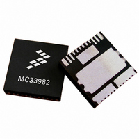
MC33982BPNA Freescale Semiconductor, MC33982BPNA Datasheet - Page 18

MC33982BPNA
Manufacturer Part Number
MC33982BPNA
Description
IC SWITCH HI SIDE SINGLE 16-PQFN
Manufacturer
Freescale Semiconductor
Type
High Sider
Datasheet
1.MC33982BPNA.pdf
(36 pages)
Specifications of MC33982BPNA
Input Type
SPI
Number Of Outputs
1
On-state Resistance
2 mOhm
Voltage - Supply
6 V ~ 27 V
Operating Temperature
-40°C ~ 125°C
Mounting Type
Surface Mount
Package / Case
16-PQFN, 16-PowerQFN
Lead Free Status / RoHS Status
Contains lead / RoHS non-compliant
Current - Output / Channel
-
Current - Peak Output
-
Available stocks
Company
Part Number
Manufacturer
Quantity
Price
Part Number:
MC33982BPNA
Manufacturer:
FREESCALE
Quantity:
20 000
POWER SUPPLY
VPWR pin. Characteristics are provided from 6.0 to 20 V for
the device. The VPWR pin supplies power to internal
regulator, analog, and logic circuit blocks. The VDD supply is
used for Serial Peripheral Interface (SPI) communication in
order to configure and diagnose the device. This IC
architecture provides a low quiescent current sleep mode.
Applying V
the Normal Mode. The device will transit to Fail-safe mode in
case of failures on the SPI (watchdog timeout).
HIGH SIDE SWITCH: HS
automotive loads with high inrush current, as well as motors
and all types of resistive and inductive loads. This N-channel
MOSFET with a 2.0 mΩ RDS(ON), is self-protected and
18
33982
FUNCTIONAL DESCRIPTION
FUNCTIONAL INTERNAL BLOCK DESCRIPTION
The 33982 is designed to operate from 4.0 to 28 V on the
This pin is the high side output controlling multiple
PWR
Power Supply
MC33982 - Functional Block Diagram
and V
SPI Interface
MCU Interface and Output Control
DD
to the device will place the device in
Power Supply
FUNCTIONAL INTERNAL BLOCK DESCRIPTION
Figure 9. Functional Internal Block Diagram
MCU Interface and Output Control
Parallel Control Inputs
presents extended diagnostics in order to detect load
disconnections and short-circuit fault conditions. The HS
output is actively clamped during a turn-off of inductive loads.
MCU INTERFACE AND OUTPUT CONTROL
MCU through the SPI. With a dedicated SPI command, it is
possible to independently turn on and off several loads that
are PWM’d at the same frequency, and duty cycles with only
one PWM signal. An analog feedback output provides a
current proportional to the load current. The SPI is used to
configure and to read the diagnostic status (faults) of high
side output. The reported fault conditions are: open load,
short-circuit to ground (OCLO-resistive and OCHI-severe
short-circuit), thermal shutdown, and under/over-voltage.
parallel input pins. The device is configured in default mode.
In Normal mode, the load is controlled directly from the
In Fail-safe mode, the load is controlled with dedicated
High Side Switch
Self-protected
Analog Integrated Circuit Device Data
High Side Switch
HS
Freescale Semiconductor


