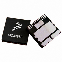
MC33982BPNA Freescale Semiconductor, MC33982BPNA Datasheet - Page 25

MC33982BPNA
Manufacturer Part Number
MC33982BPNA
Description
IC SWITCH HI SIDE SINGLE 16-PQFN
Manufacturer
Freescale Semiconductor
Type
High Sider
Datasheet
1.MC33982BPNA.pdf
(36 pages)
Specifications of MC33982BPNA
Input Type
SPI
Number Of Outputs
1
On-state Resistance
2 mOhm
Voltage - Supply
6 V ~ 27 V
Operating Temperature
-40°C ~ 125°C
Mounting Type
Surface Mount
Package / Case
16-PQFN, 16-PowerQFN
Lead Free Status / RoHS Status
Contains lead / RoHS non-compliant
Current - Output / Channel
-
Current - Peak Output
-
Available stocks
Company
Part Number
Manufacturer
Quantity
Price
Part Number:
MC33982BPNA
Manufacturer:
FREESCALE
Quantity:
20 000
While addressing this register, if the input was enabled for
direct control, a Logic [1] for the D0 bit will result in a Boolean
AND of the IN pin with its corresponding D0 message bit
when addressing the OCR register. Similarly, a Logic [0] on
the D0 pin will result in a Boolean OR of the IN pin with the
corresponding message bits when addressing the OCR
register.
independently turn on and off several loads that are PWM’d
at the same frequency and duty cycle with only one PWM
signal. This type of operation can be accomplished by
connecting the pertinent direct IN pins of several devices to a
PWM output port from the MCU, and configuring each of the
outputs to be controlled via their respective direct IN pin. The
DICR is then used to Boolean AND the direct IN(s) of each of
the outputs with the dedicated SPI bit that also controls the
output. Each configured SPI bit can now be used to enable
and disable the common PWM signal from controlling its
assigned output.
1/40000) on the CSNS pin. The default value [0] is used to
select the low ratio (C
used to select the high-speed slew rate. The default value [0]
corresponds to the low-speed slew rate.
Address 0101 — Output Switching Delay Register (OSDR)
programmable time delay that is active during Output On
transitions that are initiated via the SPI (not via direct input).
Whenever the input is commanded to transition from
Logic [0] to Logic [1], the output will be held OFF for the time
delay configured in the OSDR register.
effect on device Fail-safe mode operation. The default value
of the OSDR register is 000, equating to no delay, since the
switching delay time is 0 ms. This feature allows the user a
way to minimize inrush currents, or surges, thereby allowing
loads to be synchronously switched ON with a single
command.
Analog Integrated Circuit Device Data
Freescale Semiconductor
The DICR register is useful if there is a need to
A Logic [1] on bit D2 is used to select the high ratio (C
The OSDR register is used to configure the device with a
The programming of the contents of this register has no
SR0
, 1/5400). A Logic [1] on bit D3 is
SR1
,
times, which range from 0 to 525 ms.
Table 14. Switching Delay
Address 1101 — Watchdog Register (WDR)
watchdog timeout. Watchdog timeout is configured using bits
D1 and D0
for the desired watchdog timeout period, the WD bit (D7)
should be toggled as well to ensure that the new timeout
period is programmed at the beginning of a new count
sequence.
Table 15. Watchdog Timeout
Address 0110 — No Action Register (NAR)
packets in a daisy chain SPI configuration. This allows
devices to not be affected by commands being clocked over
a daisy-chained SPI configuration, and by toggling the WD bit
(D7) the watchdog circuitry will continue to be reset while no
programming or data readback functions are being requested
from the device.
Table 14
The WDR register is used by the MCU to configure the
The NAR register can be used to no-operation fill SPI data
OSD[2:0] (D2 : D0)
WD [1:0] (D1: D0)
shows the eight selectable output switching delay
(Table
000
001
010
011
100
101
110
111
00
01
10
11
15). When bits D1 and D0 are programmed
LOGIC COMMANDS AND REGISTERS
FUNCTIONAL DEVICE OPERATION
Turn ON Delay (ms)
Timing (ms)
2500
1250
150
225
300
375
450
525
620
310
75
0
33982
25


