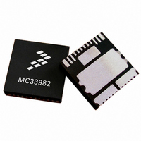
MC33982BPNA Freescale Semiconductor, MC33982BPNA Datasheet - Page 27

MC33982BPNA
Manufacturer Part Number
MC33982BPNA
Description
IC SWITCH HI SIDE SINGLE 16-PQFN
Manufacturer
Freescale Semiconductor
Type
High Sider
Datasheet
1.MC33982BPNA.pdf
(36 pages)
Specifications of MC33982BPNA
Input Type
SPI
Number Of Outputs
1
On-state Resistance
2 mOhm
Voltage - Supply
6 V ~ 27 V
Operating Temperature
-40°C ~ 125°C
Mounting Type
Surface Mount
Package / Case
16-PQFN, 16-PowerQFN
Lead Free Status / RoHS Status
Contains lead / RoHS non-compliant
Current - Output / Channel
-
Current - Peak Output
-
Available stocks
Company
Part Number
Manufacturer
Quantity
Price
Part Number:
MC33982BPNA
Manufacturer:
FREESCALE
Quantity:
20 000
Previous Address SOA[2:0] = 010
high detection level (refer to
OD2, OD1, and OD0 contain the programmed over-current
low detection levels (refer to
Table 17. Fault Register
Previous Address SOA[2:0] = 011
for the over-current fault blanking time, illustrated in
Bit OD2 reports when the over-current detection timeout
feature is active. OD3 reports whether the open load circuitry
is active.
Note The FS pin reports a fault and is reset by a new Switch-ON
command (via SPI or direct input IN).
Analog Integrated Circuit Device Data
Freescale Semiconductor
OD7 (x) = Don’t care.
OD6 (OTF) = Over-temperature Flag.
OD5 (OCHF) = Over-current High Flag. (This fault is latched.)
OD4 (OCLF) = Over-current Low Flag. (This fault is latched.)
OD3 (OLF) = Open Load Flag.
OD2 (UVF) = Under-voltage Flag. (This fault is latched or not
latched.)
OD1 (OVF) = Over-voltage Flag.
OD0 (FAULT) = This flag reports a fault and is reset by a read
operation.
OD7
The data in bit OD3 contain the programmed over-current
The data returned in bits OD1 and OD0 are current values
x
OD6
OTF
OCHF OCLF
OD5
OD4
Table
Table
OD3
OLF
12), and the data in bits
11).
OD2
UVF
OD1
OVF
Table
FAULT
OD0
13.
Previous Address SOA[2:0] =100
DICR.
Previous Address SOA[2:0] =101
• SOA3 = 0. The returned data contain the programmed
• SOA3 = 1. The returned data contain the programmed
Previous Address SOA[2:0] =110
• SOA3 = 0. OD2, OD1, and OD0 return the state of the IN,
Table 18. Pin Register
• SOA3 = 1. The returned data contains the programmed
Previous Address SOA[2:0] = 111
received, so bits OD2, OD1, and OD0 are null, or 000.
The returned data contain the programmed values in the
values in the OSDR. Bit OD3 (FSM_HS) reflects the state
of the output in the Fail-safe mode after a watchdog
timeout occurs.
values in the WDR. Bit OD2 (WDTO) reflects the status of
the watchdog circuitry. If WDTO bit is Logic [1], the
watchdog has timed out and the device is in Fail-safe
mode. If WDTO is Logic [0], the device is in Normal mode
(assuming device is powered and not in the Sleep mode),
with the watchdog either enabled or disabled.
FSI, and WAKE pins, respectively
values in the UOVR register. Bit OD1 reflects the state of
the under-voltage protection, while bit OD0 reflects the
state of the over-voltage protection (refer to
Null Data. No previous register Read Back command
IN Pin
OD2
LOGIC COMMANDS AND REGISTERS
FSI Pin
FUNCTIONAL DEVICE OPERATION
OD1
(Table
18).
WAKE Pin
Table
OD0
16).
33982
27


