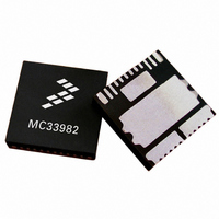
MC33982BPNA Freescale Semiconductor, MC33982BPNA Datasheet - Page 24

MC33982BPNA
Manufacturer Part Number
MC33982BPNA
Description
IC SWITCH HI SIDE SINGLE 16-PQFN
Manufacturer
Freescale Semiconductor
Type
High Sider
Datasheet
1.MC33982BPNA.pdf
(36 pages)
Specifications of MC33982BPNA
Input Type
SPI
Number Of Outputs
1
On-state Resistance
2 mOhm
Voltage - Supply
6 V ~ 27 V
Operating Temperature
-40°C ~ 125°C
Mounting Type
Surface Mount
Package / Case
16-PQFN, 16-PowerQFN
Lead Free Status / RoHS Status
Contains lead / RoHS non-compliant
Current - Output / Channel
-
Current - Peak Output
-
Available stocks
Company
Part Number
Manufacturer
Quantity
Price
Part Number:
MC33982BPNA
Manufacturer:
FREESCALE
Quantity:
20 000
Table 10. Serial Input Address and Configuration Bit
DEVICE REGISTER ADDRESSING
addresses and their impact on device operation.
Address x000 — Status Register (STATR)
the various configuration register contents without disrupting
the device operation or the register contents. The register bits
D2, D1, and D0 determine the content of the first eight bits of
SO data. In addition to the device status, this feature provides
the ability to read the content of the OCR, SOCHLR,
CDTOLR, DICR, OSDR, WDR, NAR, and UOVR registers.
(Refer to the section entitled
(Device Status Return Data)
Address x001 — Output Control Register (OCR)
through the SPI. Incoming message bit D0 (IN_SPI) reflects
the desired states of the high-side output: a Logic [1] enables
the output switch and a Logic [0] turns it OFF. A Logic [1] on
message bit D1 enables the Current Sense (CSNS) pin. Bits
D2 and D3 must be Logic [0]. Bit D7 is used to feed the
watchdog if enabled.
Address x010 — Select Over-current High and Low
Register (SOCHLR)
output over-current low and high detection levels,
respectively. In addition to protecting the device, this slow
blow fuse emulation feature can be used to optimize the load
requirements to match system characteristics. Bits D2 : D0
are used to set the over-current low detection level to one of
24
33982
x = Don’t care.
FUNCTIONAL DEVICE OPERATION
LOGIC COMMANDS AND REGISTERS
SOCHLR
CDTOLR
Register
STATR
OSDR
UOVR
TEST
The following section describes the possible register
The STATR register is used to read the device status and
The OCR register allows the MCU to control the output
The SOCHLR register allows the MCU to configure the
DICR
WDR
OCR
NAR
SI
D7 D6 D5 D4
Map
x
x
x
x
x
0
1
0
1
x
0
0
0
0
1
1
1
1
1
1
0
0
1
1
0
0
0
1
1
1
0
1
0
1
0
1
1
0
0
1
OL_dis CD_dis
SOCH
Serial Input Data
FAST
SR
D3
Serial Output Communication
beginning on page 26.)
0
0
0
0
0
0
Freescale Internal Use (Test)
SOCL2
CSNS
SOA2
OSD2
high
D2
0
0
0
0
SOCL1
OCLT1
UV_dis
CSNS
SOA1
OSD1
IN dis
WD1
EN
D1
0
SOCL0
OV_dis
IN_SPI
OCLT0
SOA0
OSD0
WD0
A/O
D0
0
eight possible levels as defined in
set the over-current high detection level to one of two levels
as defined in
Table 11. Over-current Low Detection Levels
Table 12. Over-current High Detection Levels
Address x011 — Current Detection Time and Open Load
Register (CDTOLR)
the amount of time the device will allow an over-current low
condition before output latches OFF occurs. Bits D1 and D0
allow the MCU to select one of four fault blanking times
defined in
the over-current low detection levels. If the selected over-
current high level is reached, the device will latch off within
20 μs
Table 13. Over-current Low Detection Blanking Time
(CD_dis) detection timeout feature. A Logic [1] on bit D3
disables the open load (OL) detection feature.
Address x100 — Direct Input Control Register (DICR)
or configure the direct IN pin control of the output. A Logic [0]
on bit D1 will enable the output for direct control by the IN pin.
A Logic [1] on bit D1 will disable the output from direct control.
SOCL2
(D2)
The CDTOLR register is used by the MCU to determine
A Logic [1] on bit D2 disables the over-current low
The DICR register is used by the MCU to enable, disable,
0
0
0
0
1
1
1
1
.
SOCH (D3)
OCLT [1:0]
Table
SOCL1
0
1
(D1)
0
0
1
1
0
0
1
1
Table
00
01
10
11
13. Note that these timeouts apply only to
12.
SOCL0
(D0)
0
1
0
1
0
1
0
1
Analog Integrated Circuit Device Data
Over-current High Detection
Over-current Low Detection
Table
Freescale Semiconductor
(Amperes)
(Amperes)
11. Bit D3 is used to
150
100
155 ms
Timing
1.2 ms
150 μ s
10 ms
50
45
40
35
30
25
20
15


