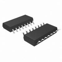
SG6980SZ Fairchild Semiconductor, SG6980SZ Datasheet - Page 14

SG6980SZ
Manufacturer Part Number
SG6980SZ
Description
IC PFC CTRLR AVERAGE CURR 16SOP
Manufacturer
Fairchild Semiconductor
Datasheet
1.SG6980SZ.pdf
(18 pages)
Specifications of SG6980SZ
Mode
Average Current
Frequency - Switching
65kHz
Current - Startup
10µA
Voltage - Supply
12.5 V ~ 20 V
Operating Temperature
-20°C ~ 125°C
Mounting Type
Surface Mount
Package / Case
16-SOIC (3.9mm Width)
Output Voltage
0.3 V to 25 V
Switching Frequency
68 KHz
Operating Temperature Range
- 20 C to + 125 C
Mounting Style
Through Hole
Duty Cycle (max)
98 %
Lead Free Status / RoHS Status
Lead free / RoHS Compliant
Available stocks
Company
Part Number
Manufacturer
Quantity
Price
Part Number:
SG6980SZ
Manufacturer:
SG
Quantity:
20 000
Single-Stage PFC Controller
Protections & Built-in Latch Circuit
The SG6980 provides full protection functions to prevent
the power supply and the load from being damaged. The
protection features include:
PFC Feedback Over-Voltage Protection. When the PFC
feedback voltage exceeds the over-voltage threshold, the
SG6980 inhibits the PFC switching signal. This
protection prevents the PFC power converter from
operating abnormally while the FB pin is open.
PFC Feedback Under-Voltage Protection. The SG6980
stops the PFC switching signal whenever the PFC
feedback voltage drops below the under-voltage threshold.
This protection feature is designed to prevent the PFC
power converter from experiencing abnormal conditions
while the FB pin is shorted to ground.
VDD Over-Voltage Protection. The built-in clamping
circuit clamps V
over-voltage threshold.
RI Pin Open / Short Protection. The RI pin is used to set
the switching frequency and internal current reference. If
the RI pin is short or open, SG6980 is off.
PCB Layout
SG6980 has a single ground pin. High sink currents in the
output therefore cannot be returned separately. Good
high-frequency or RF layout practices should be followed.
Avoid long PCB traces and component leads. Locate
decoupling capacitors near the SG6980. A resistor of 5 ~
20 : is recommended, connecting in series from the
output to the gate of the MOSFET.
Isolating the interference between the PFC and PWM
stages is also important. Figure 7 shows an example of the
PCB layout. The ground trace 1 is connected from the
ground pin to the decoupling capacitor, which should be
low impedance and as short as possible. The ground trace
© System General Corp.
Version 1.0.1 (IAO33.0064.B0)
DD
whenever the V
DD
voltage exceeds the
- 14 -
2 provides a signal ground. It should be connected directly
to the decoupling capacitor C
The ground trace 3 is independently tied from the
decoupling capacitor to the PFC output capacitor C
ground in the output capacitor C
reference for power switching. To provide a good ground
reference and reduce the switching noise of both the PFC
and PWM stages, the ground traces 6 and 7 should be
located very near and be low impedance.
The ICS pin is connected directly to R
improve noise immunity. (Beware that it may incorrectly
be connected to the ground trace 2). The IMP and IPK
pins should also be connected directly, via the resistors R
and R
P
, to another terminal of R
www.sg.com.tw • www.fairchildsemi.com
FIG. 7 PCB Layout
DD
Product Specification
S
and/or to the ground pin.
.
O
is the major ground
September 17, 2007
S
through R
SG6980
O
. The
3
to
2


