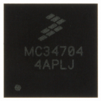
MC34704AEP Freescale Semiconductor, MC34704AEP Datasheet - Page 17

MC34704AEP
Manufacturer Part Number
MC34704AEP
Description
IC POWER MANAGEMENT 56-QFN
Manufacturer
Freescale Semiconductor
Datasheet
1.MC34704BEPR2.pdf
(54 pages)
Specifications of MC34704AEP
Applications
Processor
Current - Supply
86mA
Voltage - Supply
2.7 V ~ 5.5 V
Operating Temperature
-20°C ~ 85°C
Mounting Type
Surface Mount
Package / Case
56-QFN
Output Voltage
5 V
Input Voltage
2.7 V to 5.5 V
Switching Frequency
750 KHz to 2 MHz
Mounting Style
SMD/SMT
Number Of Outputs
8
Lead Free Status / RoHS Status
Lead free / RoHS Compliant
REG5 BOOST STAGE BOOTSTRAP CAPACITOR
INPUT PIN (BT5U)
pin to enhance the gate of the Switch Power MOSFET.
REG4 BUCK STAGE BOOTSTRAP CAPACITOR
INPUT PIN (BT4D)
pin to enhance the gate of the Switch Power MOSFET.
REG4 POWER SUPPLY INPUT VOLTAGE (PVIN4)
FET. Input decoupling /filtering is required for proper REG4
operation.
REG4 BUCK STAGE SWITCHING NODE (SW4D)
pin.
REG4 REGULATED OUTPUT VOLTAGE PIN
(VOUT4)
to the pin as possible.
REG4 BOOST STAGE SWITCHING NODE (SW4U)
pin.
REG4 BOOST STAGE BOOTSTRAP CAPACITOR
INPUT PIN (BT4U)
pin to enhance the gate of the Switch Power MOSFET.
REG4 VOLTAGE FEEDBACK INPUT FOR
VOLTAGE REGULATION/PROGRAMMING (FB4)
REG4 COMPENSATION NETWORK CONNECTION
(COMP4)
REG3 BOOTSTRAP CAPACITOR INPUT PIN (BT3)
to enhance the gate of the Switch Power MOSFET.
REG3 POWER SUPPLY INPUT VOLTAGE (PVIN3)
FET. Input decoupling /filtering is required for proper REG3
operation.
Analog Integrated Circuit Device Data
Freescale Semiconductor
Connect a 1.0 μF capacitor between this pin and SW5U
Connect a 0.01 μF capacitor between this pin and SW4D
This is the connection to the drain of the high side switch
The inductor is connected between this pin and the SW4U
Connect this pin to the load and to the output filter as close
The inductor is connected between this pin and the SW4D
Connect a 0.01 μF capacitor between this pin and SW4U
Connect the feedback resistor divider to this pin.
REG4 compensation network connection.
Connect a 0.01 μF capacitor between this pin and SW3 pin
This is the connection to the drain of the high side switch
FUNCTIONAL PIN DESCRIPTION
REG3 SWITCHING NODE (SW3)
regulated REG3 output.
REG3 OUTPUT VOLTAGE RETURN PIN (VOUT3)
REG3 VOLTAGE FEEDBACK INPUT FOR
VOLTAGE REGULATION/PROGRAMMING (FB3)
SOFT START TIME (SS)
connecting this pin to an external resistor divider between
VDDI and AGND pins.
OSCILLATOR FREQUENCY (FREQ)
this pin to an external resistor divider between VDDI and
AGND pins. This pin sets F
REG8 VOLTAGE FEEDBACK INPUT FOR
VOLTAGE REGULATION/PROGRAMMING (FB8)
voltage mode control is used. When current mode control is
used, connect this pin between the LED string and an I
resistor to GND to force the operating current. Refer to
Figure 10
REG8 BOOTSTRAP CAPACITOR INPUT PIN (BT8)
to enhance the gate of the Synchronous Power MOSFET.
REG8 REGULATED OUTPUT VOLTAGE PIN
(VOUT8)
output filter as close to the pin as possible.
REG8 SWITCHING NODE (SW8)
REG1 SWITCHING NODE (SW1)
REG1 REGULATED OUTPUT VOLTAGE BEFORE
THE CUT-OFF SWITCH (VG)
This supplies the internal circuits and the gate drive.
The inductor is connected between this pin and the
This is the discharge path of REG3 output voltage.
Connect the feedback resistor divider to this pin.
The soft start time for all regulators can be adjusted by
The oscillator frequency can be adjusted by connecting
Connect the feedback resistor divider to this pin, when
Connect a 0.01 μF capacitor between this pin and SW8 pin
Connect this pin directly to the load directly and to the
The inductor is connected between this pin and VIN pin.
The inductor is connected between this pin and VIN pin.
REG1 regulated output voltage before the cutoff switch.
and
Figure
11. Exclude the components not used.
SW1
FUNCTIONAL PIN DESCRIPTION
value.
FUNCTIONAL DESCRIPTION
SET
34704
17


