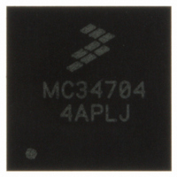
MC34704AEP Freescale Semiconductor, MC34704AEP Datasheet - Page 44

MC34704AEP
Manufacturer Part Number
MC34704AEP
Description
IC POWER MANAGEMENT 56-QFN
Manufacturer
Freescale Semiconductor
Datasheet
1.MC34704BEPR2.pdf
(54 pages)
Specifications of MC34704AEP
Applications
Processor
Current - Supply
86mA
Voltage - Supply
2.7 V ~ 5.5 V
Operating Temperature
-20°C ~ 85°C
Mounting Type
Surface Mount
Package / Case
56-QFN
Output Voltage
5 V
Input Voltage
2.7 V to 5.5 V
Switching Frequency
750 KHz to 2 MHz
Mounting Style
SMD/SMT
Number Of Outputs
8
Lead Free Status / RoHS Status
Lead free / RoHS Compliant
Regulator 3 (Synchronous Buck - internally
compensated)
• L: A buck power stage can be designed to operate in CCM
• C
step during the current rising time and is define as:
44
34704
FUNCTIONAL DEVICE OPERATION
COMPONENT CALCULATION
L
Δ
dtI
1. Define I
L
The passive components associated to these frequencies are calculated with the following formulas
On the 34704 V
for load currents above a certain level usually 5 to 15% of
full load. The minimum value of inductor to maintain CCM
can be determined by using the following procedure:
min
contribute to its impedance and output voltage ripple are
the ESR, the ESL and the capacitance C. A good
approach to calculate the minimum real capacitance
needed is to include the transient response analysis to
control the maximum overshoot as desired.
• First calculate the dt_I (inductor current rising time)
Where the parameter
C1
C2
R2
R3
C3
Iostep
min
OUT
15% of full load.
given by:
=
≥
=
=
=
=
=
≥
: The three elements of output capacitor that
(
------------------------------------------------------------------------------------------------------------- -
---------------------
Δ
Vo
Io
D′T
------------------
V
⎛
⎝
⎛
⎝
⎛
⎝
⎛
⎝
Vin
Iostep
----------------------------- -
2π F
----------------------------- -
2π F
----------------------------- -
2π F
----------------------------- -
2π F
max
=
RAMP
+
OB
----------- -
2I
(
(
(
(
min
⎛
⎝
Vo
Io
D
------------- -
T
Fsw
OB
1
1
Z2
Z1
1
P1
1
P2
as the minimum current to maintain CCM as
max
max
⎛
⎜
⎝
---------------- -
D′
R1
C1
C2
R2
RAMP
⎞ Vin
⎠
min
(
1
R
⎛
⎝
)
)
)
)
⎞
⎠
⎞
⎠
⎞
⎠
⎞
⎠
-------------------------------
DSONLSFET
2
is half of 1.2 V since each operation mode spends only half the ramp.
⎞
⎟
⎠
Δ
⎛
⎝
min
IO
2I
------------------------------ -
2π F
L
OB
_
(
–
step is the maximum current
Vo
PO
1
⎞
⎠
R1
+
R
)
⎞
⎠
L
) D′
(
min
[H]
[s]
)T
[A]
overshoot expressed as a percentage of the output voltage,
typically from 3 to 5% of Vo.
• R1 and RB: These two resistors help to set the output
Regulator 8 (Synchronous Boost - internally
compensated -Voltage or current feedback)
maximum current of 30 mA and can be used with voltage
ESR
RB
C
• Then the output capacitor can be chosen as follow:
Where
• Finally find the maximum allowed ESR to allow the
voltage to the desire value using a V
between 10 k and 100 K and then calculate RB as follows:
REG8 is a Synchronous Boost converter set to 15V with a
OUT
NOTE: do not use the parameters
indistinctly, the first one indicates the output voltage rip-
ple, while the second one is the maximum output volt-
age overshoot (transient response).
desired transient response:
=
max
≤
--------------------- -
----------- -
Vref
Δ
Vo
Io
----------------------
Δ
=
VO
R1
Vo
max
Δ
------------------------------------- -
–
Vo 1
max
max
Vo
1
dtI
(
r
is the maximum allowed transient
(
Fsw
–
D
Analog Integrated Circuit Device Data
min
) L ( )
)
Freescale Semiconductor
REF
Δ
VO
=0.6 V, select R1
R
and
[Ω]
[Ω]
[F]
Δ
VO
max


